Microwave module having converter for improving transmission characteristics
- Summary
- Abstract
- Description
- Claims
- Application Information
AI Technical Summary
Benefits of technology
Problems solved by technology
Method used
Image
Examples
Example
COMPARATIVE EXAMPLE 1
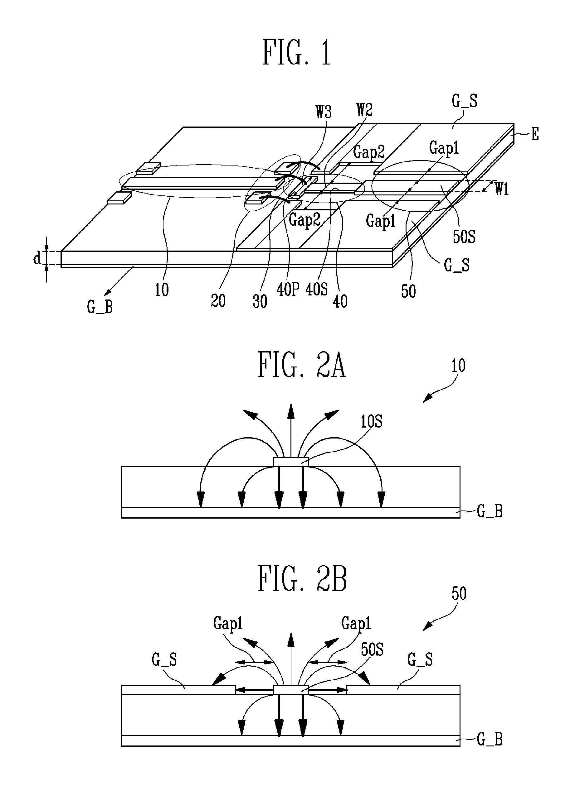
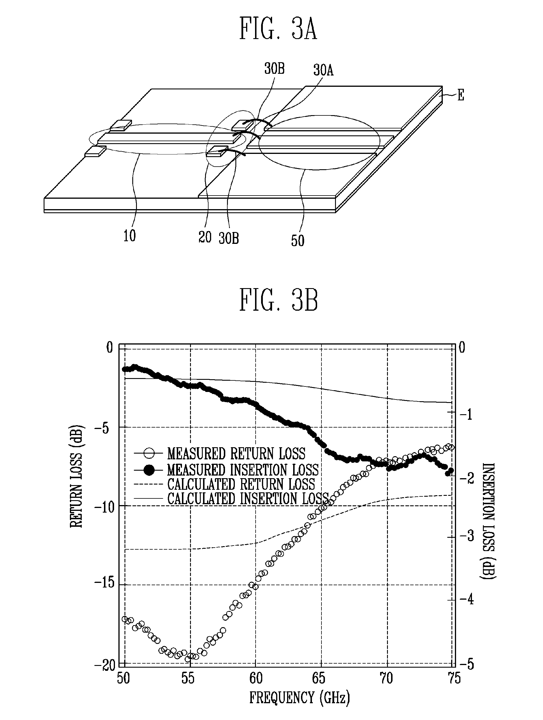
[0037]FIG. 3A is a perspective view of a microstrip transmission line 10 and a CBCPW transmission line 50 connected by general wire bonding, and FIG. 3B is a graph showing the result obtained by measuring transmission and reflection characteristics of bonded lines of FIG. 3A using a network analyzer. In the measurement, a dielectric substrate having a permittivity of 5.8 and a thickness of 100 μm, the 50-ohm microstrip transmission line 10, and the 50-ohm CBCPW transmission line 50 were used.
[0038]As illustrated in FIG. 3A, the microstrip transmission line 10 and the CBCPW transmission line 50 are connected through one ribbon 30A having a width of 50 μm and a thickness of 13 μm, and two wires 30B having a diameter of 20 μm. In this case, according to transmission characteristics in a millimeter-wave band, insertion loss and return loss are caused by a change in impedance due to the ribbon 30A and the bonding wires 30B and difference in electric field distributio...
Example
COMPARATIVE EXAMPLE 2
[0041]FIG. 4A is a perspective view of a microstrip transmission line 10 and a CBCPW transmission line 50 connected through bonding wires 30 in which a converter 40 consisting of a bonding pad 40P alone is employed, and a width W3 of the bonding pad 40P is increased. And, FIG. 4B is a graph showing an experimental result of transmission characteristics obtained from the structure of FIG. 4A while the width W3 of the bonding pad 40P is changed by a multiple of the width of the CBCPW transmission line 50.
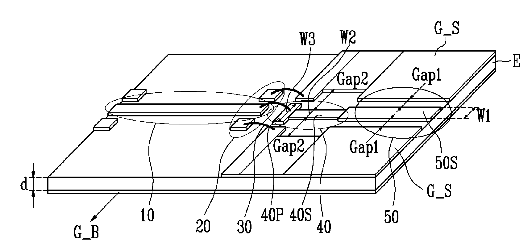
[0042]As illustrated in FIG. 4A, when the width W3 of the bonding pad 40P increases, the capacitance components of the bonding pad 40P increase in number, and thus the insertion loss and return loss of the bonding wires 30 decrease slightly but not significantly, as shown in FIG. 4B. In particular, when the width W3 of the bonding pad 40P significantly increases, the insertion loss and return loss increase again. Consequently, it is preferable to have an appropria...
Example
COMPARATIVE EXAMPLE 3
[0044]FIG. 5A is a perspective view of a microstrip transmission line 10 and a CBCPW transmission line 50 connected through bonding wires 30 in which a converter 40 consisting of a signal line 40S alone is employed, and a distance between the signal line 40S and side grounds G_S is changed. And, FIG. 5B is a graph showing a simulated result of transmission characteristics obtained from the structure of FIG. 5A while the distance between the signal line 40S of the converter 40 and the side grounds G_S is changed by a multiple of a thickness d of a dielectric substrate.
[0045]As illustrated in FIG. 5A, when the distance between the signal line 40S in the converter 40 and the side grounds G_S increases, transmission loss decreases, but not significantly. In particular, when the distance between the signal line 40S and the side grounds G_S is more than double the thickness d of the dielectric substrate, the transmission characteristics are almost unchanged.
EXEMPLARY ...
PUM
 Abstract
Description
Claims
Application Information


