Method for improving the bonding properties of microstructured substrates, and devices prepared with this method
a microstructured substrate and bonding technology, applied in the direction of pretreatment surfaces, biological testing, synthetic resin layered products, etc., can solve the problems of difficult manipulation of large microchannel arrays, complex lithographic steps of devices, and high construction and operation costs of such chips, so as to facilitate the deformation of surfaces, shorten the embossing time, and reduce the deformation.
- Summary
- Abstract
- Description
- Claims
- Application Information
AI Technical Summary
Benefits of technology
Problems solved by technology
Method used
Image

Examples
example 1
Preparation of a Rigid Template with Microstructures of Thicknesses from 20 to 50 μm for the Subsequent Preparation of Embossed Substrates.
[0169]Glass slides, with largest dimension ranging from 5 cm to 30 cm were cleaned in acid “piranha” solution (75% H2SO4 and 25% H2O2) for 30 minutes, rinsed in de-ionized water and air-dried. The slides were dehydrated in a convection oven at 150° C. Dry resist films (SY355), were bought from Elga Europe. The PE layer was cut to the size of the glass, peeled off and the resist was laminated on the clean glass substrate using a hot-roll office laminator (Catena 35 roll laminator, General Binding Corporation, USA) under UV-free conditions.
[0170]A mask with tie microfluidic pattern was printed on a transparency film using a high-resolution printer. The laminated resist (while still retaining the PET layer on top) was exposed through the mask using a UV lamp (refs 66057 and 68808 from Oriel Instruments). Following exposure, the PET layer was peeled ...
example 2
Preparation of a Large-Scale Flexible Template for the Preparation of Substrates According to the Invention by a Roll Lamination Process.
[0171]A process following the same lines as presented in example 1, except for the difference quoted below:
[0172]200 μm thick PET film of format A4 was used as the support for the microstructures instead of glass slides.
[0173]The PET film was cleaned ultrasonically in acetone and isopropanol.
[0174]The resist was laminated on the cleaned PET film under the same conditions as the glass substrate and UV exposure of the microchannel pattern was carried out for 20 seconds.
[0175]Since PET has a glass transition temperature of 69° C., the exposed film was baked on a hot-plate at 95° C. for only 30 s to facilitate better sticking of resist on PET.
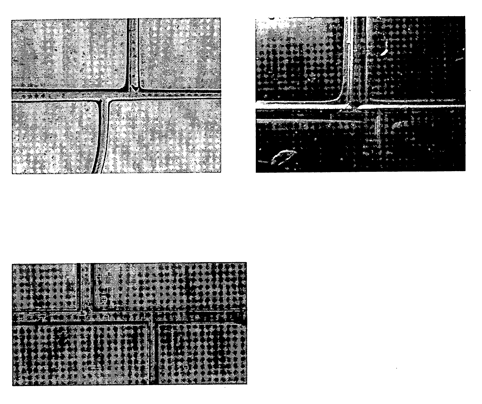
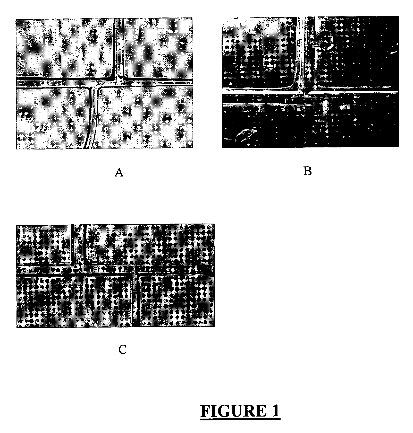
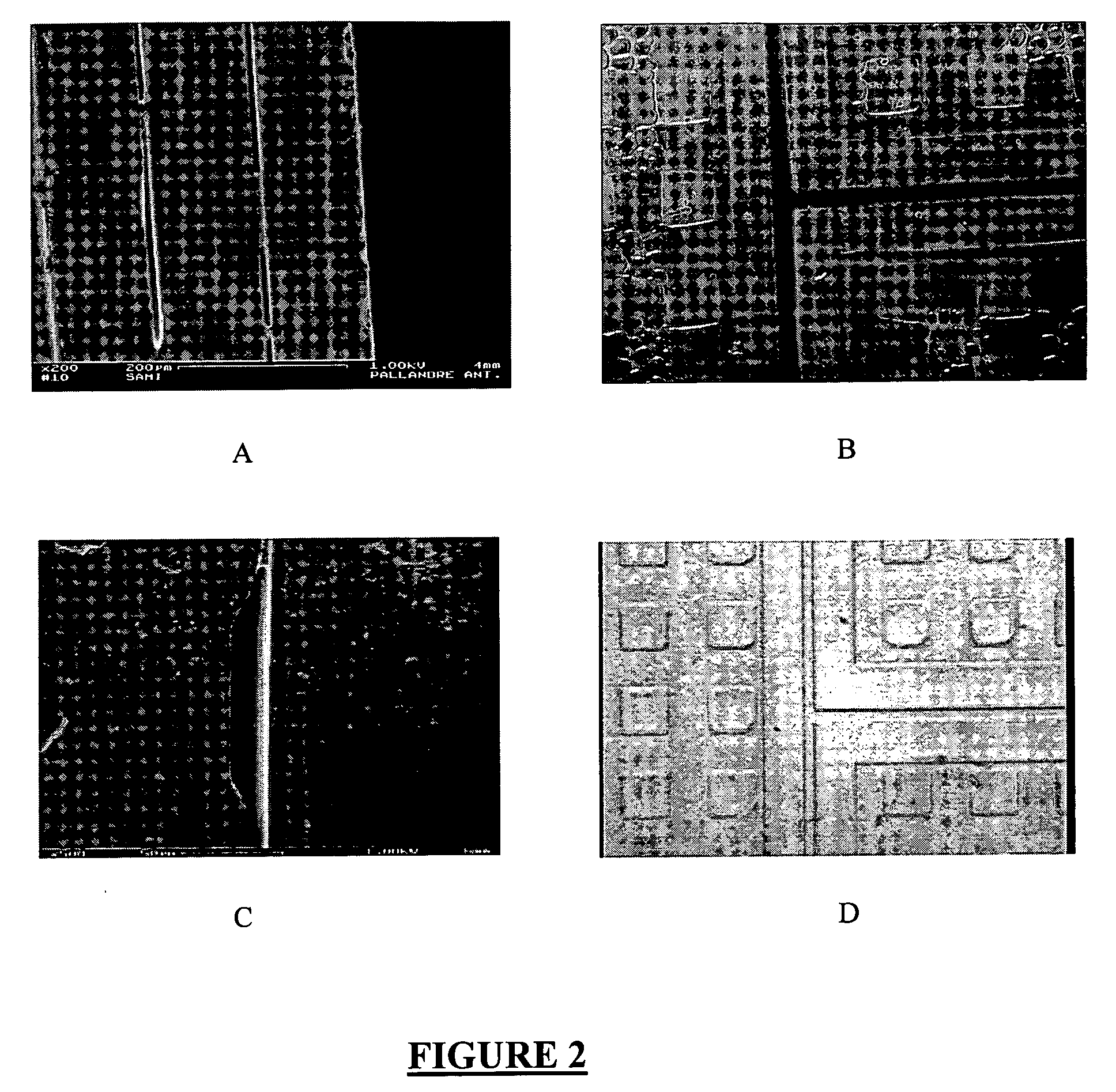
[0176]The pattern was developed as before using the BMR developer, rinsed using BMR rinser and dried by airjet. The resulting “master” is displayed in FIG. 1A.
example 4
Improvement of the Preparation of Substrates in Thermoplastic Polymer, using a Pretreatment with a Composition According to the Invention.
[0179]The process follows this of example 3, except for the following differences.
[0180]Prior to the lamination process, a freshly-prepared 10% (v / v) mixture of hexadecane (a plasticizer of COC) in isopropanol (a poor solvent of COC) was poured on one side of the COC film wing a pipette and the excess solvent was removed using a Kimwipe® after 1 mn. The solvent was allowed to be absorbed by COC by leaving the film in air till there was no liquid on the surface. Then, the COC film was laminated following the same protocol as in example 3, taking care that the face of the film treated with the solvent mixture faces the template. The shape of the channel, presented in FIG. 1C, is improved with regards to those prepared according to example 3 (FIG. 1B).
[0181]This replication protocol can be applied to other thermoplastic polymers, by adapting the preh...
PUM
| Property | Measurement | Unit |
|---|---|---|
| glass transition temperature | aaaaa | aaaaa |
| radius of gyration | aaaaa | aaaaa |
| depth | aaaaa | aaaaa |
Abstract
Description
Claims
Application Information
 - R&D Engineer
- R&D Manager
- IP Professional
- Industry Leading Data Capabilities
- Powerful AI technology
- Patent DNA Extraction
Browse by: Latest US Patents, China's latest patents, Technical Efficacy Thesaurus, Application Domain, Technology Topic.
© 2024 PatSnap. All rights reserved.Legal|Privacy policy|Modern Slavery Act Transparency Statement|Sitemap