Organic light emitting display and fabricating method thereof

a light-emitting display and organic technology, applied in the field can solve the problems of difficult fabrication of organic light-emitting display having a thickness below 1 mm, low yield of production, and greatly increased fabrication process time, so as to enhance the rigidity of the product, not easily damaged by external force, and the effect of enhancing the rigidity

Inactive Publication Date: 2008-06-19
SAMSUNG DISPLAY CO LTD
View PDF48 Cites 31 Cited by
  • Summary
  • Abstract
  • Description
  • Claims
  • Application Information

AI Technical Summary

Benefits of technology

[0013]Another object of the present invention is to prevent the bending and damage of the substrate during the fabricating process.
[0067]As noted above, in the method of fabricating an organic light emitting display according to the present invention, since an anti-friction layer is formed on a substrate, when bonding two substrates, damage to the substrate is prevented by preventing contact with a metal formed on the substrate or the surface of the substrate.

Problems solved by technology

However, in the present organic light emitting displays, since a protective layer technology that can substitute for an encapsulation technology has not been sufficiently developed, it is difficult to fabricate an organic light emitting display having a thickness below 1 mm.
However, the above-noted fabricating method has a problem in that the fabricating process time greatly increases because after the semiconductor layer or the organic light emitting diode is formed on the respective glass substrates, the glass substrates are bonded to each other and are etched or ground.
Moreover, such a conventional fabricating method has a problem in that the yield of production is low and the fabricating cost is expensive because the partly finished glass substrates are bonded to each other and the glass substrate, the semiconductor layer and the organic light emitting diode is damaged during bonding process.
However, such a fabricating method has a problem in that the glass substrate bends or contacts a moving device and is damaged during the moving process because the glass substrate is very thin.

Method used


Image

  • Organic light emitting display and fabricating method thereof
  • Organic light emitting display and fabricating method thereof
  • Organic light emitting display and fabricating method thereof

Examples


Embodiment Construction

[0075]Hereinafter, the exemplary embodiment of the present invention is explained in detail below with reference to the attached drawings so that the present invention is derived by a person having ordinary skill in the field to which the present invention belongs.

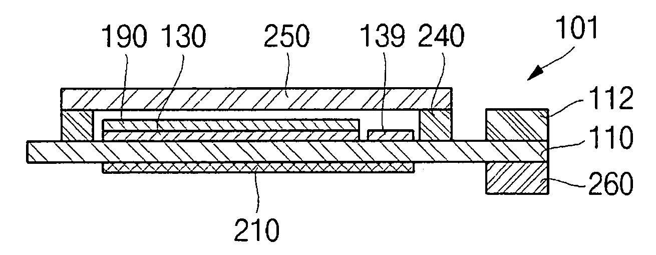
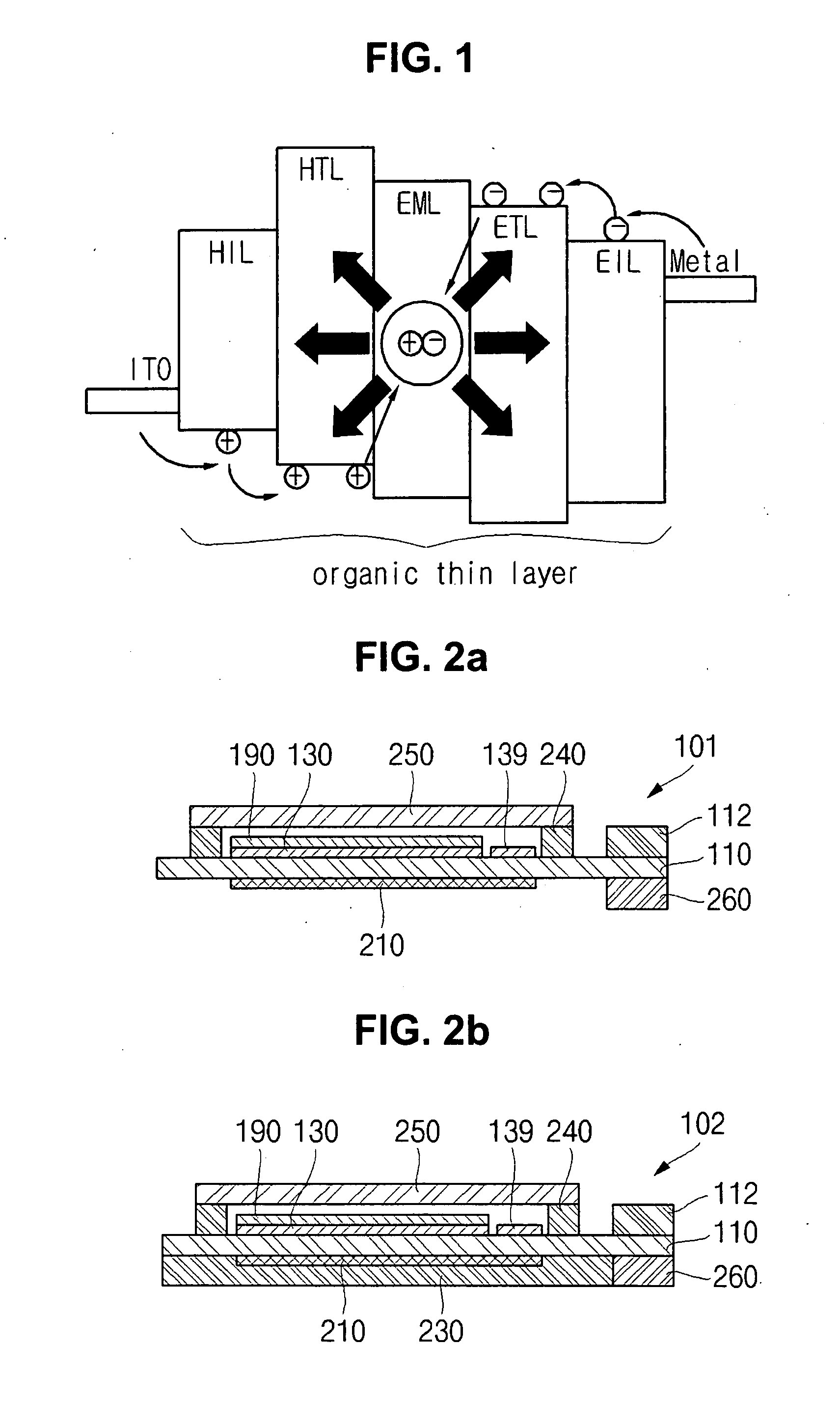
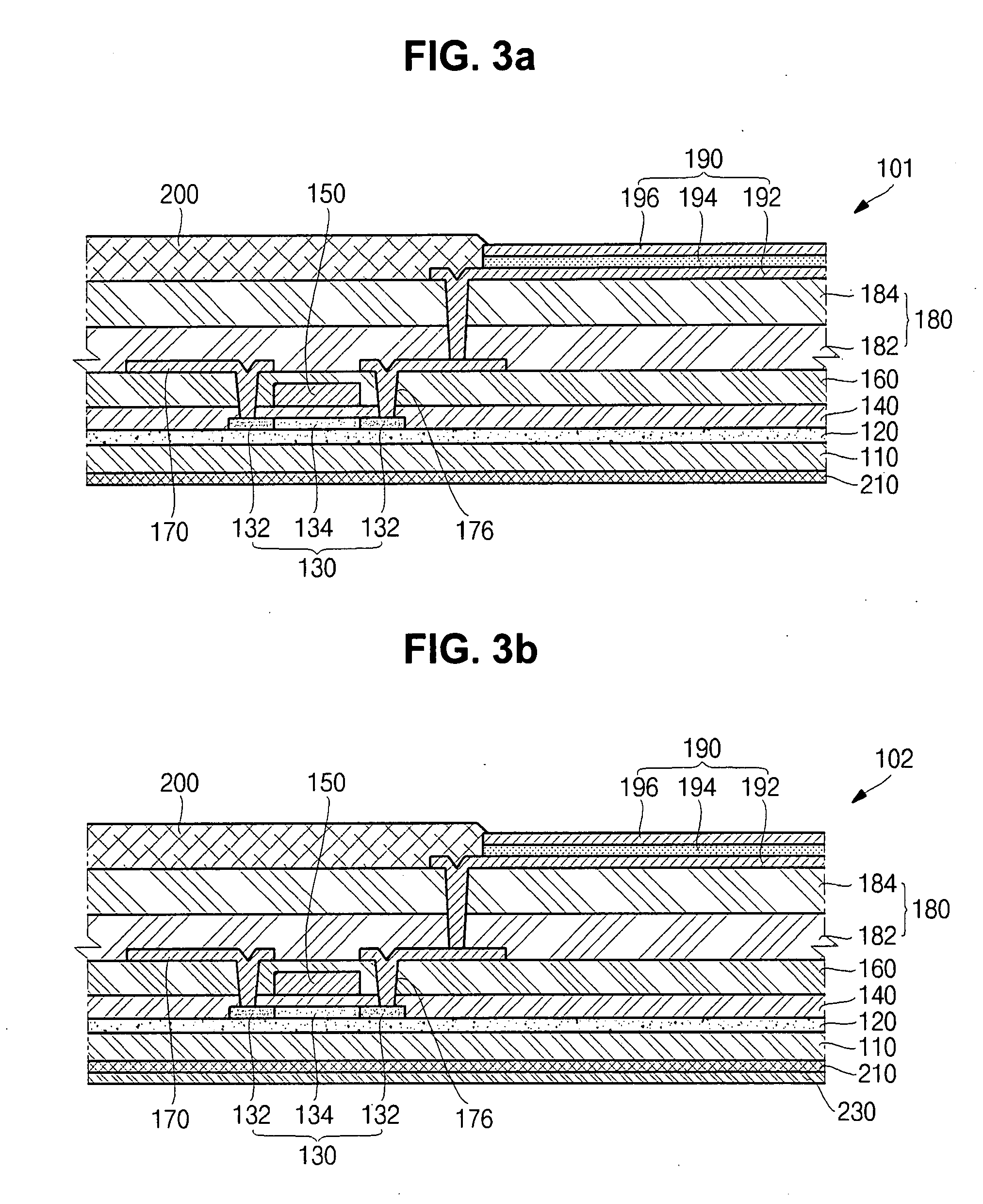
[0076]FIG. 2a and FIG. 2b are cross-sections of an organic light emitting display according to an embodiment of the present invention.

[0077]As illustrated in FIG. 2a, an organic light emitting display 101 according to an embodiment of the present invention includes a substrate 110, a semiconductor layer 130 formed on the substrate 110, a driving circuit 139 formed on one side of the semiconductor layer 130, an organic light emitting diode 190 formed on the semiconductor layer 130, an encapsulant 240 formed on an upper periphery of the substrate 110 which is the outer perimeter of the organic light emitting diode 190, the semiconductor layer 130 and the driving circuit 139, and an encapsulation substrate 250 attached to the...


PUM


Abstract

An organic light emitting display including a substrate, a semiconductor layer formed on the substrate, an organic light emitting diode formed on the semiconductor layer, an encapsulant formed on a periphery of the substrate which is an outer periphery of the organic light emitting diode and the semiconductor layer; and an encapsulation substrate attached to the encapsulant.

Description

CLAIM OF PRIORITY[0001]This application makes reference to, incorporates the same herein, and claims all benefits accruing under 35 U.S.C.§119 from an application for ORGANIC LIGHT EMITTING DISPLAY AND FABRICATING METHOD THEREOF earlier filed in the Korean Intellectual Property Office on the 13th day of Dec. 2006 and there duly assigned Serial No. 10-2006-0127290.BACKGROUND OF THE INVENTION[0002]1. Field of the Invention[0003]The present invention relates to an organic light emitting display and a fabrication method thereof and, more particularly, the present invention relates to a thin organic light emitting display having a reduced fabricating process time and can prevent a substrate from being bent and damaged during the fabricating process.[0004]2. Description of the Related Art[0005]Generally, an organic light emitting display self-emits light by causing an electric current to flow through a fluorescent or phosphorescent organic compound and allowing an electron and a hole to b...

Claims


Application Information

Patent Timeline
Patent Type & Authority Applications(United States)
IPC IPC(8): H01L51/50
CPCH01L51/0097H01L2251/5338H01L51/56H01L51/5237H10K77/111H10K50/841H10K2102/311H10K71/00H05B33/02H05B33/10H10K50/84
Inventor KIM, JONGYUNCHOI, BYOUNGDEOG
Owner SAMSUNG DISPLAY CO LTD
Why Eureka
Try Eureka