

Radio frequency identification device
a radio frequency identification and receiver technology, applied in the direction of near-field systems using receivers, read/write/interrogation/identification systems, instruments, etc., can solve the problems of rfid b>30/b> having the possibility of failing to detect the transmission rate and disable the adjustment of the reception bandwidth, so as to reduce the influence
- Summary
- Abstract
- Description
- Claims
- Application Information
AI Technical Summary
Benefits of technology
Problems solved by technology
Method used
Image

Examples
embodiment 1
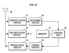
[0045]FIG. 6 is a block diagram illustrating an RFID 30 according to an embodiment of the present invention.
[0046]The RFID 30 is comprised of a demodulation circuit 31, a rectification circuit 32 and a modulation circuit 33, each of which is connected to an antenna 38. The RFID 30 is further comprised of a decoding circuit 34 connected to the demodulation circuit 31, a coding circuit 35 connected to the modulation circuit 33, a control unit 36 connected to the decoding circuit 34 and the coding circuit 35, and a nonvolatile memory 37 connected to the control unit 36. These elements 31-37 are built into an IC chip.
[0047]The rectification circuit 32 serves as a generation source of supply voltage necessary for operating the RFID 30. In the memory 37, such information as a system identifier and an RFID identifier is stored. A command received by the antenna 38 is converted into a binary signal through the demodulation circuit 31 as will be described later, decoded into digital data (co...
embodiment 2
[0069]FIG. 10 shows a block diagram of a demodulation circuit applied to the RFID according to a second embodiment of the present invention.
[0070]The demodulation circuit 31 of the second embodiment is provided with a plurality of LPFs different in the reception bandwidth to each other, which are connected to the output circuit of the detector 300. Here, it is assumed that the reader / writer 10 transmits each command as an amplitude-modulated signal at a transmission rate of 40 kbps, 80 kbps, or 160 kbps. In this case, the output signal S300 of the detector 300 is supplied to a first LPF 311A with an 80-kHz reception bandwidth, a second LPF 311B with a 160-kHz reception bandwidth, and a third LPF 311C with a 320-kHz reception bandwidth. The output signals of LPFs 311A, 311B and 311C are converted into the binary signals 310A, 310B, and 310C through binarization circuits 312A, 312B, and 312C, respectively.
[0071]In the present embodiment, the binary signals 310A, 310B, and 310C are inp...
embodiment 3
[0079]FIG. 12 shows a block diagram of a demodulation circuit applied to the RFID according to a third embodiment of the present invention.
[0080]The demodulation circuit 31 of the third embodiment includes, at the output circuit of the detector 300, a first LPF 311A, a second LPF 311B, and a third LPF 311C different in the reception bandwidth to each other, and binarization circuits 312A, 312B, and 312C, similarly to the second embodiment. Here, as in the second embodiment, it is assumed that the reader / writer 10 transmits each command as an amplitude-modulated signal at the transmission rate of 40 kbps, 80 kbps, or 160 kbps. In this case, the reception bandwidths of the first LPF 311A, the second LPF 311B, and the third LPF 311C become 80 kHz, 160 kHz, and 320 kHz, respectively.
[0081]In the present embodiment, the binary signals 310A, 310B, and 310C are inputted into the transmission rate detection circuit 313. During the receiving period of the preamble (or frame sync) of Command ...
PUM
 Abstract
Description
Claims
Application Information