

Semiconductor device for detecting flow rate of fluid
a technology of fluid flow rate and semiconductor device, which is applied in the direction of liquid/fluent solid measurement, instruments, material moisture content, etc., can solve the problem of error only by the amount of moisture content, and achieve the effect of reducing the dimensions of the device, improving the and improving detection accuracy of flow ra
- Summary
- Abstract
- Description
- Claims
- Application Information
AI Technical Summary
Benefits of technology
Problems solved by technology
Method used
Image

Examples
first embodiment
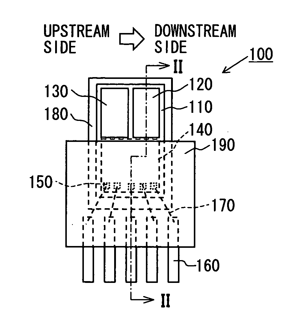
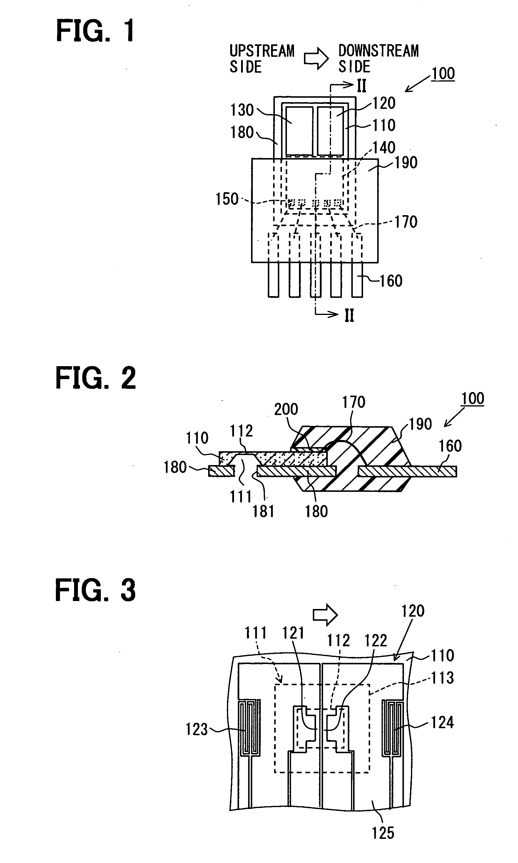
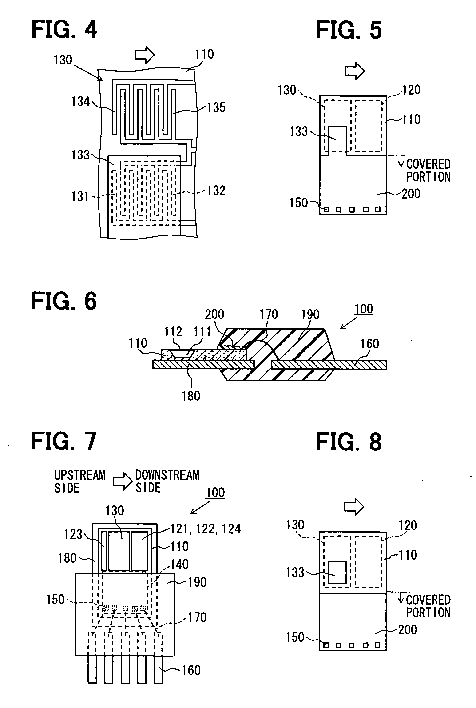
[0028]FIG. 1 is a plan view showing a schematic configuration of a semiconductor device of a first embodiment of the present disclosure. FIG. 2 is a schematic cross section taken along line II-II of FIG. 1. FIG. 3 is an enlarged plan view of a portion around a flow sensor. FIG. 4 is an enlarged plan view of a portion around a humidity sensor. FIG. 5 is a schematic plan view showing the positional relation between a moisture sensitive film and a high polymer film over a semiconductor substrate. In FIG. 2, for convenience, a flow sensor and a circuit part are not shown. In FIGS. 3 and 4, for convenience, insulating films such as a protection film are not shown. In the following diagrams, a hollow arrow expresses the flow direction of a fluid in normal times.
[0029]As shown in FIGS. 1 and 2, on a semiconductor substrate 110, a flow sensor 120 for sensing a flow rate of fluid and a humidity sensor 130 for sensing humidity of the fluid are formed as main components of a semiconductor devi...
second embodiment
[0049]A second embodiment of the present disclosure will be described with reference to FIGS. 8 and 9. FIG. 8 is a schematic plan view showing the positional relation between a moisture sensitive film and a high polymer film over the semiconductor substrate in a semiconductor device of the second embodiment. FIG. 9 is a schematic cross section of the semiconductor device. FIG. 9 corresponds to FIG. 2 showing the first embodiment and, for convenience like in FIG. 2, a flow sensor and a circuit part are not shown.
[0050]Since the semiconductor device of the second embodiment is largely common to that of the first embodiment, the detailed description of the common parts will not be repeated hereinbelow, and different parts will be described with concentration. The same reference numerals are designated to the same elements as those of the first embodiment.
[0051]In the first embodiment, an example of integrating the moisture sensitive film 133 and the high polymer film 200 was described....
third embodiment
[0057]A third embodiment of the present disclosure will now be described with reference to FIG. 10. FIG. 10 is a plan view showing a schematic configuration of a semiconductor device of the third embodiment, and corresponds to FIG. 1 showing the first embodiment.
[0058]Since the semiconductor device of the third embodiment is largely common to that of the first embodiment, the detailed description of the common parts will not be repeated hereinbelow, and different parts will be described with concentration. The same reference numerals are designated to the same elements as those of the first embodiment.
[0059]In the first embodiment, the flow sensor 120 and the humidity sensor 130 are formed side by side along the fluid flow direction on the same side of the semiconductor substrate 110, and the humidity sensor 130 is provided on the upstream side of the flow sensor 120. On the other hand, the third embodiment is characterized by the point that, as shown in FIG. 10, the humidity sensor...
PUM
 Abstract
Description
Claims
Application Information