Electron Blocking Layers for Electronic Devices

Inactive Publication Date: 2008-06-26
SANDISK TECH LLC
View PDF99 Cites 19 Cited by
  • Summary
  • Abstract
  • Description
  • Claims
  • Application Information

AI Technical Summary

Benefits of technology

[0006]Described herein are non-volatile memory devices and a method of making a memory device that may provide advantages over existing devices and methods.

Problems solved by technology

However, Al2O3 does not completely block charge transport and leads to program and erase saturation at lower voltage windows.

Method used


Image

  • Electron Blocking Layers for Electronic Devices
  • Electron Blocking Layers for Electronic Devices
  • Electron Blocking Layers for Electronic Devices

Examples


Embodiment Construction

Introduction

[0027]It should be appreciated that the particular implementations shown and described herein are exemplary and are not intended to otherwise limit the scope of the present invention in any way. Indeed, for the sake of brevity, conventional electronics, manufacturing, semiconductor devices, and other functional aspects of the systems (and components of the individual operating components of the systems) may not be described in detail herein.

[0028]It should be understood that the spatial descriptions (e.g., “above,”“below,”“up,”“down,”“top,”“bottom,” etc.) made herein are for purposes of illustration only, and that devices described herein can be spatially arranged in any orientation or manner.

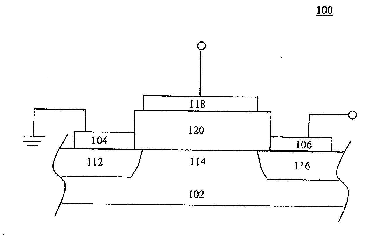
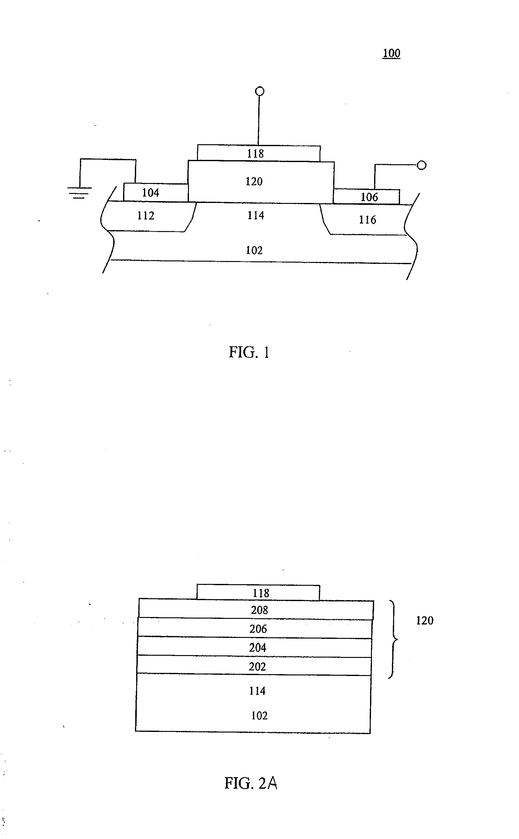
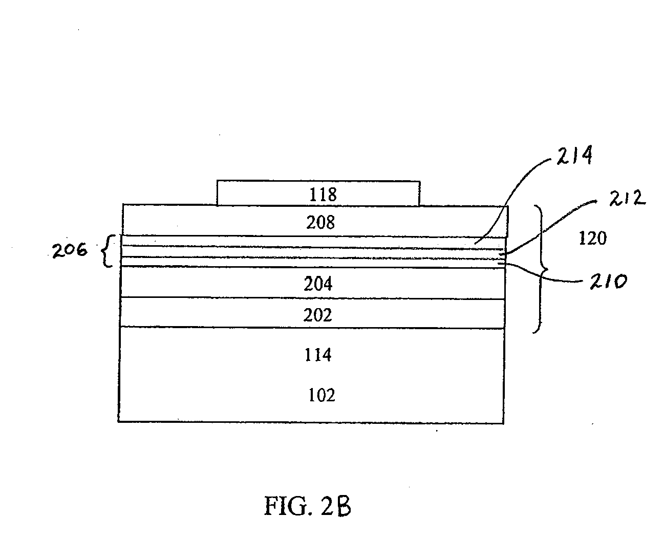
[0029]The terms “adjacent,”“on,”“over,” and “overlying,” as used herein to describe the relationship of one layer to another layer, are intended to be interpreted broadly to include layers in direct contact with one another and layers spaced apart by one or more intervening layers. ...


PUM


Abstract

Methods and apparatuses for electronic devices such as non-volatile memory devices are described. The memory devices include a multi-layer control dielectric, such as a double or triple layer. The multi-layer control dielectric includes a combination of high-k dielectric materials such as aluminum oxide (Al2O3), hafnium oxide (HfO2), and/or hybrid films of hafnium aluminum oxide. The multi-layer control dielectric provides enhanced characteristics, including increased charge retention, enhanced memory program/erase window, improved reliability and stability, with feasibility for single or multistate (e.g., two, three or four bit) operation.

Description

CROSS-REFERENCE TO RELATED APPLICATIONS[0001]The present application is a continuation-in-part of U.S. patent application Ser. No. 11 / 641,956, filed on Dec. 20, 2006, the entire contents of which are hereby incorporated by reference.TECHNICAL FIELD[0002]The present disclosure relates to memory devices, and more particularly, to flash memory devices.BACKGROUND[0003]Non-volatile memory devices, such as flash memory devices, are memory devices that can store information even when not powered. A flash memory device stores information in a charge storage layer that is separated from a “control gate.” A voltage is applied to the control gate to program and erase the memory device by causing electrons to be stored in, and discharged from the charge storage layer.[0004]A control dielectric is used to isolate the control gate from the charge storage layer. It is desirable for the control dielectric to block charge flow between the charge storage layer and control gate. High-k dielectric laye...

Claims


Application Information

Patent Timeline
Patent Type & Authority Applications(United States)
IPC IPC(8): H01L29/792H01L21/336
CPCH01L29/42332H01L29/7881H01L29/517
Inventor CHEN, JIANDUAN, XIANGFENGCRUDEN, KARENLIU, CHAONALLABOLU, MADHURI L.RANGANATHAN, SRIKANTHLEON, FRANCISCOPARCE, J. WALLACE
Owner SANDISK TECH LLC
Why Eureka
Try Eureka