Automated optimization of VLSI layouts for regularity

a technology of automatic optimization and layout, applied in the direction of total factory control, instruments, computing, etc., can solve the problems of unavoidable vlsi manufacturing, significant increase in the processing required to create photolithographic masks, and shrinking dimensions of deep-submicron vlsi, so as to reduce the pattern space of difficult patterns, improve lithographic fidelity, and increase the regularity of design

Inactive Publication Date: 2008-06-26
GLOBALFOUNDRIES INC
View PDF5 Cites 8 Cited by
  • Summary
  • Abstract
  • Description
  • Claims
  • Application Information

AI Technical Summary

Benefits of technology

[0006]The invention addresses these and other problems associated with the prior art by attempting to improve lithographic fidelity via reducing the pattern space of difficult patterns or structures in a design layout for an integrated circuit design, and thereby increasing the regularit

Problems solved by technology

The shrinking dimensions of deep-submicron VLSI typically require extremely precise and time-consuming post-design lithographic processing in order to achieve correct on-wafer geometric structures.
Wafer features in fact have shrunken below the resolution of the tooling used to create the lithographic masks that are used to form the features on a wafer, resulting in a significant increase in the processing necessary to create photolithographic masks.
As a consequence of these shrinking dimensions, certain problems associated with the lithographic process, such as line-end foreshortening and corner rounding, have become unavoidable in VLSI manufacture.
However, corrections that are performed to address some issues (e.g., bridging/shorts) can exacerbate other issues (e.g., pinching/opens), and as a result, careful tradeoffs often must be made when attempting to tune the lithographic process.
Importantly, it has been found that similar but

Method used


Image

  • Automated optimization of VLSI layouts for regularity
  • Automated optimization of VLSI layouts for regularity
  • Automated optimization of VLSI layouts for regularity

Examples


Embodiment Construction

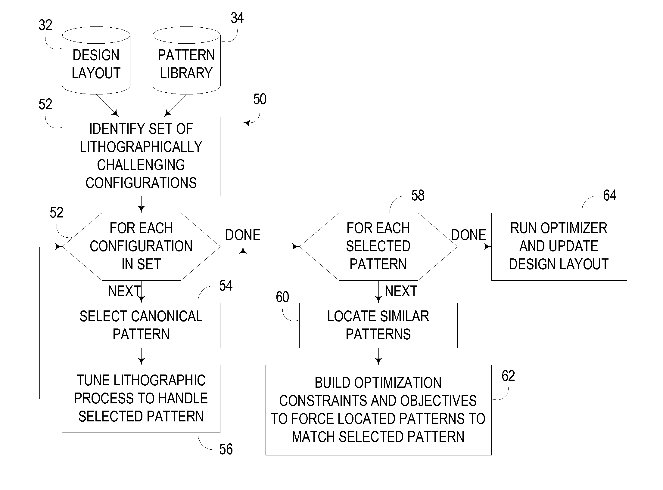
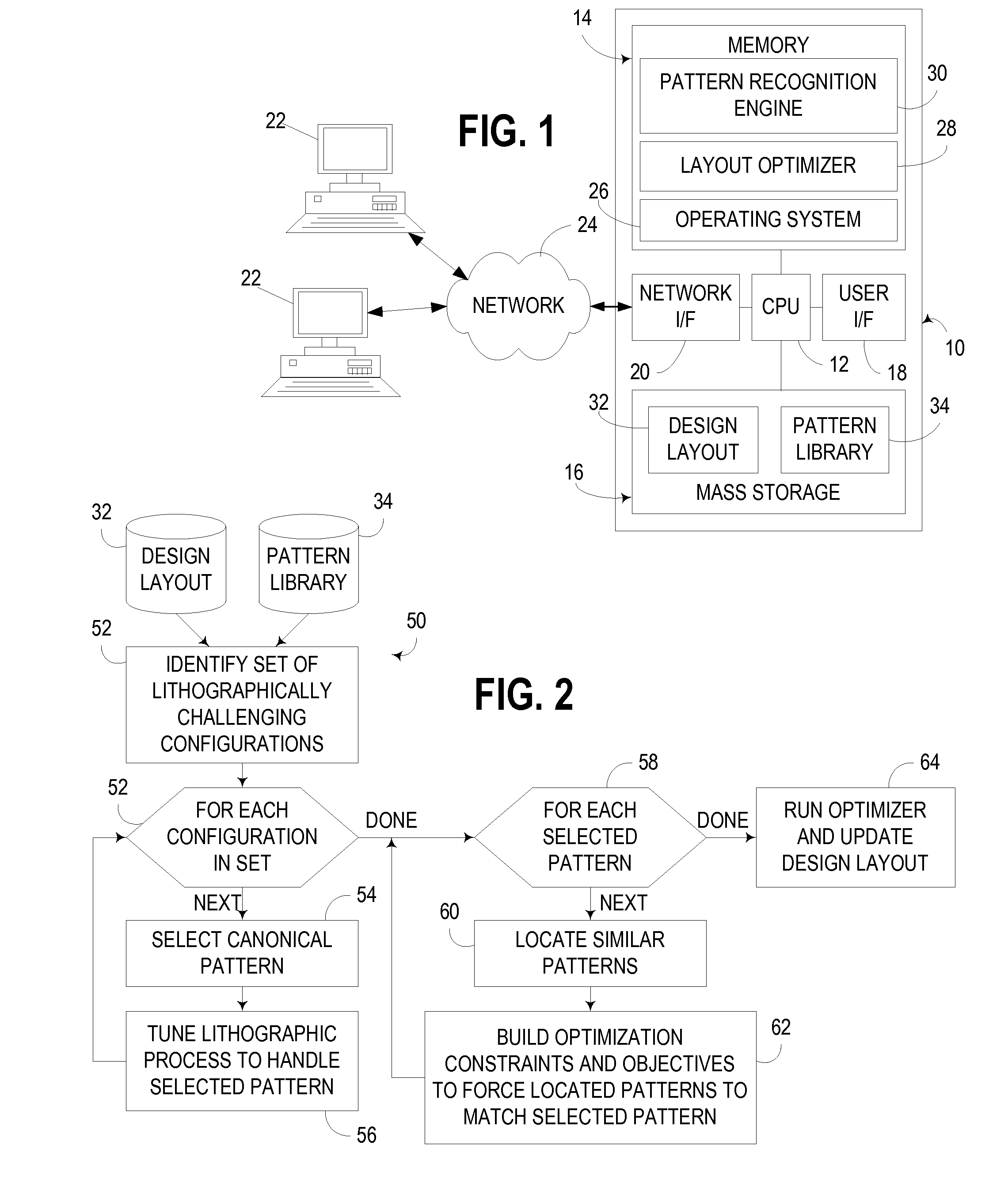
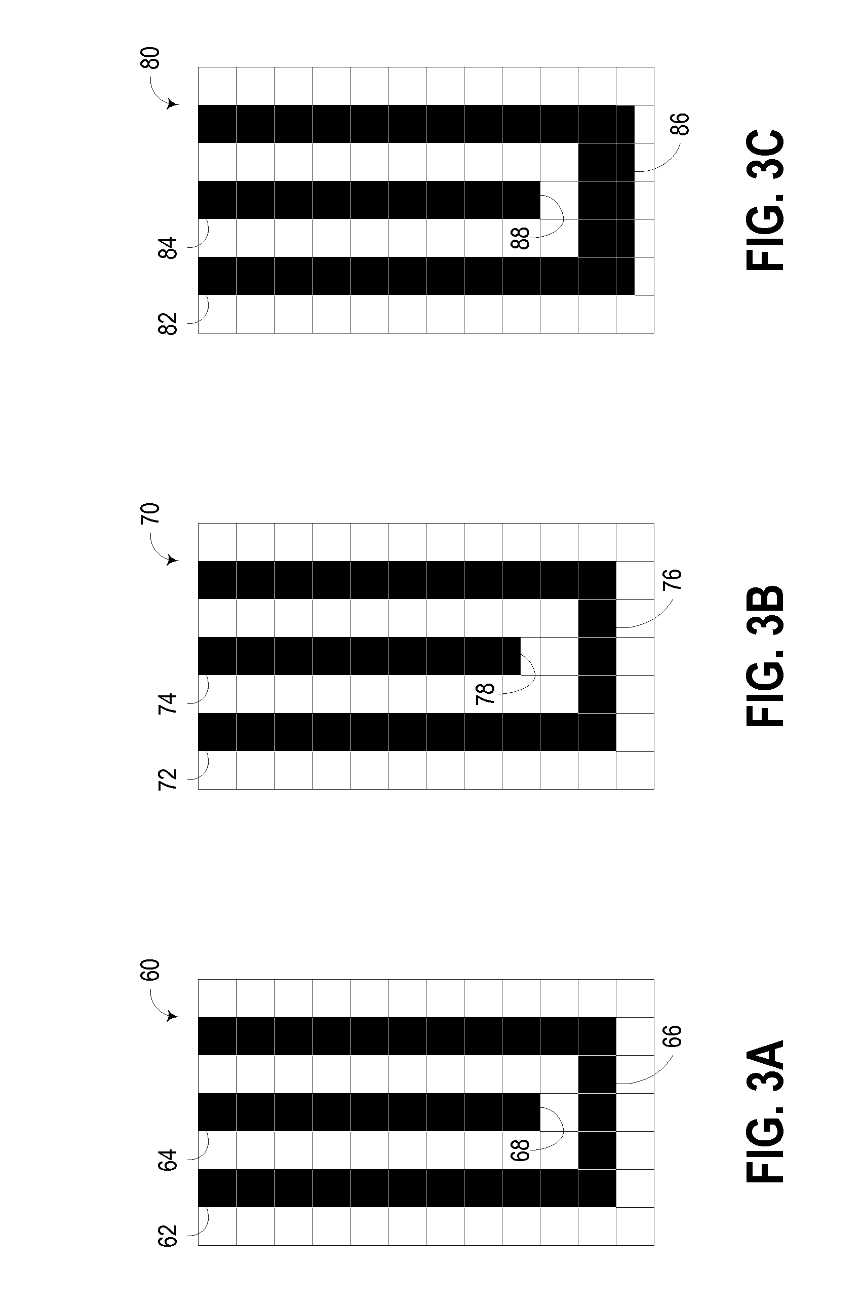
[0012]The embodiments described hereinafter improve lithographic fidelity via reducing the pattern space of difficult patterns or structures in a design layout for an integrated circuit design. Among other benefits, the embodiments herein are suitable for use with existing design layouts or physical designs, as well as design layouts incorporating substantial custom (e.g., non-building block or non-library element) features. The pattern space of difficult patterns or structures is reduced by converting similar patterns to selected canonical geometric configurations, such that lithographic processing can then be tuned to handle a smaller set of patterns.

[0013]In particular, embodiments consistent with the invention operate upon an existing VLSI physical design, or design layout, and identify therein a set of lithographically challenging configurations or patterns. For each such configuration or pattern, a canonical geometric configuration is selected, and the lithographic process is ...


PUM


Abstract

VLSI lithographic fidelity is improved via reducing the pattern space of difficult patterns or structures in a design layout for an integrated circuit design, and thereby increasing the regularity of the design, by converting patterns or structures that are similar but not identical to one another into a smaller set of canonical geometric configurations. By doing so, lithographic processing can be tuned to handle the smaller set of configurations more accurately and efficiently.

Description

FIELD OF THE INVENTION[0001]The invention is generally directed to the design and fabrication of semiconductor integrated circuits.BACKGROUND OF THE INVENTION[0002]The shrinking dimensions of deep-submicron VLSI typically require extremely precise and time-consuming post-design lithographic processing in order to achieve correct on-wafer geometric structures. Wafer features in fact have shrunken below the resolution of the tooling used to create the lithographic masks that are used to form the features on a wafer, resulting in a significant increase in the processing necessary to create photolithographic masks. This processing is known as optical proximity correction (OPC). As a consequence of these shrinking dimensions, certain problems associated with the lithographic process, such as line-end foreshortening and corner rounding, have become unavoidable in VLSI manufacture.[0003]Many of the issues inherent in photolithography can be addressed during the lithographic process, princi...

Claims


Application Information

Patent Timeline
IPC IPC(8): G06F17/50
CPCG06F2217/12G06F17/5081G06F30/398G06F2119/18Y02P90/02
Inventor CHIDAMBARRAO, DURESETICULP, JAMES A.HIBBELER, JASON D.
Owner GLOBALFOUNDRIES INC
Why Eureka
Try Eureka