Method of combining floating body cell and logic transistors

a floating body cell and logic transistor technology, applied in the direction of transistors, semiconductor devices, electrical apparatus, etc., can solve the problems of difficult structure fabrication, low back gate voltage, and low back gate voltag

Inactive Publication Date: 2008-07-03
INTEL CORP
View PDF6 Cites 39 Cited by
  • Summary
  • Abstract
  • Description
  • Claims
  • Application Information

AI Technical Summary

Problems solved by technology

One problem with this arrangement is the relatively high voltage required on the back gate because of the thick oxide.
If the oxi

Method used


Image

  • Method of combining floating body cell and logic transistors
  • Method of combining floating body cell and logic transistors
  • Method of combining floating body cell and logic transistors

Examples


Embodiment Construction

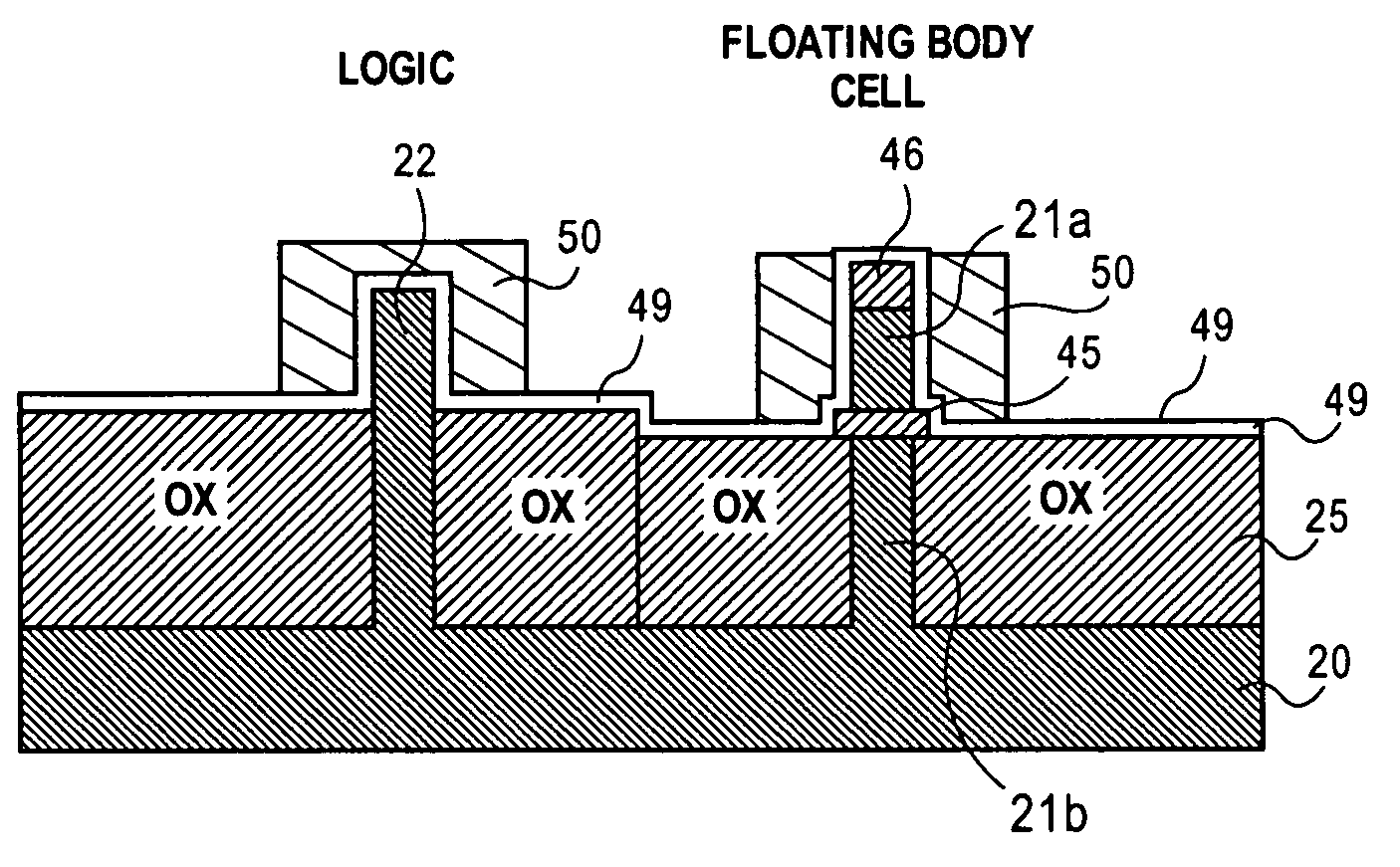
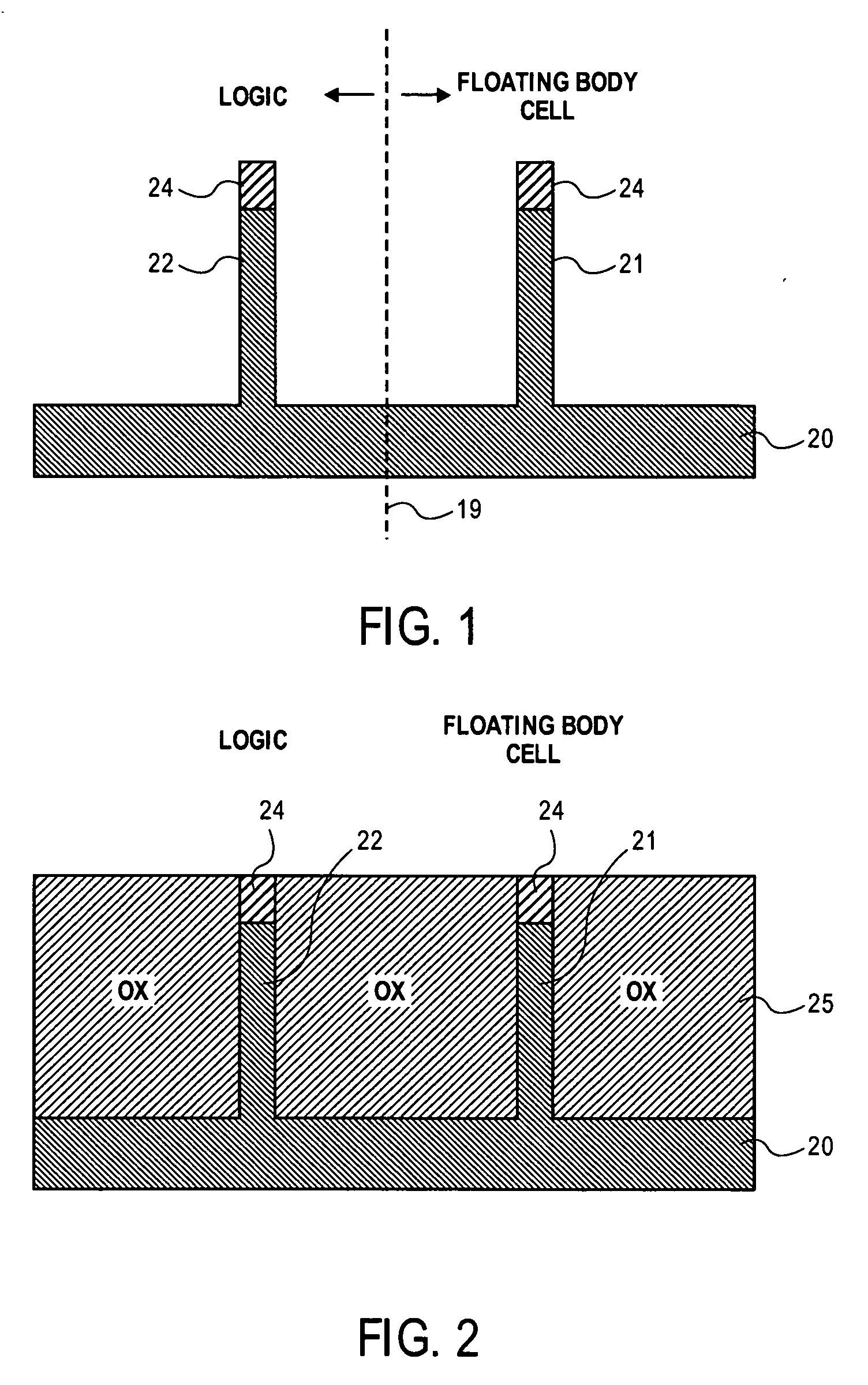
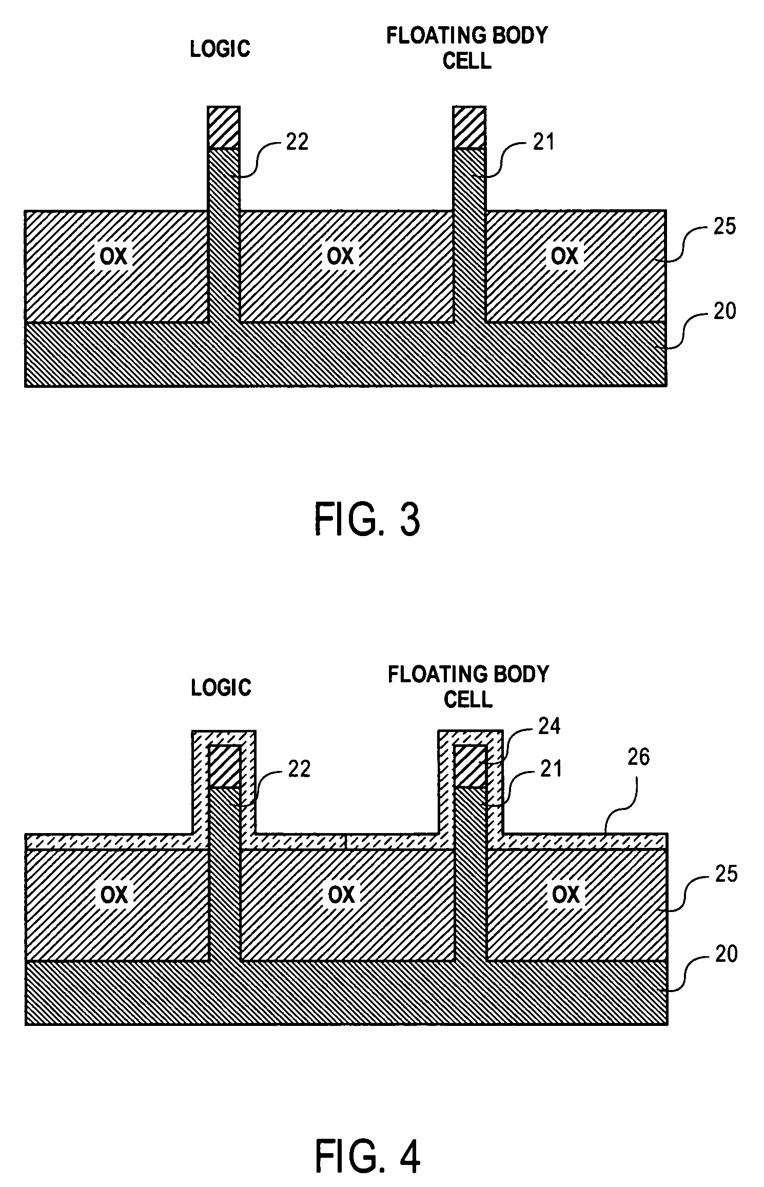
[0020]In the following description, memory devices, more specifically floating body memory cells (FBCs), and a method for fabricating the cells on a bulk substrate which includes logic devices, is described. Numerous specific details are set forth to provide a thorough understanding of the present invention. It will be apparent to one skilled in the art, that the present invention may be practiced without these specific details. In other instances, well-known processing steps such as cleaning and etching steps, are not described in detail to avoid unnecessarily obscuring the present invention.

[0021]Referring to FIG. 1, a monocrystalline silicon substrate 20 is illustrated in a cross-sectional, elevation view after the fins or bodies 21 and 22 have been etched from the substrate. The etching process typically includes the formation of a pad oxide, not illustrated, and the formation of a silicon nitride layer. The nitride layer is patterned to form the masking members 24, allowing the...


PUM


Abstract

An integrated circuit having both floating body cells and logic devices fabricated in a bulk silicon substrate is described. The floating body cells have electrically floating bodies formed by oxidizing a lower portion of the cell bodies to electrically isolate them from the substrate.

Description

FIELD OF THE INVENTION[0001]The invention relates to the field of fabricating floating body memory cells and logic devices on a common substrate, and the resultant integrated circuit.PRIOR ART AND RELATED ART[0002]Most common dynamic random-access memory (DRAM) cells store charge on a capacitor and use a single transistor for accessing the capacitor. More recently, a cell has been proposed which stores charge in a floating body of a transistor. A back gate is biased to retain charge in the floating body. A front gate is used to sense the presence or absence of charge by determining the voltage threshold and to write data into the cell.[0003]In one proposal, an oxide layer is formed on a silicon substrate and a silicon layer for the active devices is formed on the oxide layer (SOI substrate). The floating bodies are defined from the silicon layer; the substrate is used as a back or biased gate. One problem with this arrangement is the relatively high voltage required on the back gate...

Claims


Application Information

Patent Timeline
IPC IPC(8): H01L21/336H01L29/788
CPCH01L21/84H01L29/7841H01L27/1203H01L27/10802H10B12/20
Inventor DOYLE, BRIAN S.DATTA, SUMANKAVALIEROS, JACKCHAU, ROBERT
Owner INTEL CORP
Why Eureka
Try Eureka