Supercharge Your Innovation With Domain-Expert AI Agents!

TEG pattern and method for testing semiconductor device using the same

a semiconductor device and test element technology, applied in semiconductor/solid-state device testing/measurement, semiconductor/solid-state device details, instruments, etc., can solve the problems of affecting affecting the efficiency of semiconductor device development, so as to improve the yield of semiconductor devices and promote the effect of the development of them

Inactive Publication Date: 2008-07-03
DONGBU HITEK CO LTD
View PDF7 Cites 7 Cited by
  • Summary
  • Abstract
  • Description
  • Claims
  • Application Information

AI Technical Summary

Benefits of technology

[0015]Also, the embodiments of the present invention provide a TEG pattern and a method for testing a semiconductor device capable of improving the yield of the semiconductor device and promoting the efficiency of the development thereof through a newly devised two-terminal TEG.

Problems solved by technology

In such a measurement process, the wafer of the semiconductor device may be damaged.
As a result, one may be incapable of monitoring characteristics of an actual wafer in process (e.g., during the manufacturing process or between steps of the process, while the wafer is still in the manufacturing fab).
However, the related art may not sufficiently control a margin for the overlay misalignment in 90 nm technology node or less, thereby leading to a possible increase in leakage current.
However, in manufacturing the semiconductor device on a 90 nm tech node or less according to the related art, an electric test module, which can effectively monitor the degree of overlay misalignment of a metal 1 contact (M1C) in the active area, and a test module, which can accurately monitor the leakage characteristics of the PN junction diode area, may not have systemically been developed.

Method used


Image

  • TEG pattern and method for testing semiconductor device using the same
  • TEG pattern and method for testing semiconductor device using the same
  • TEG pattern and method for testing semiconductor device using the same

Examples


first embodiment

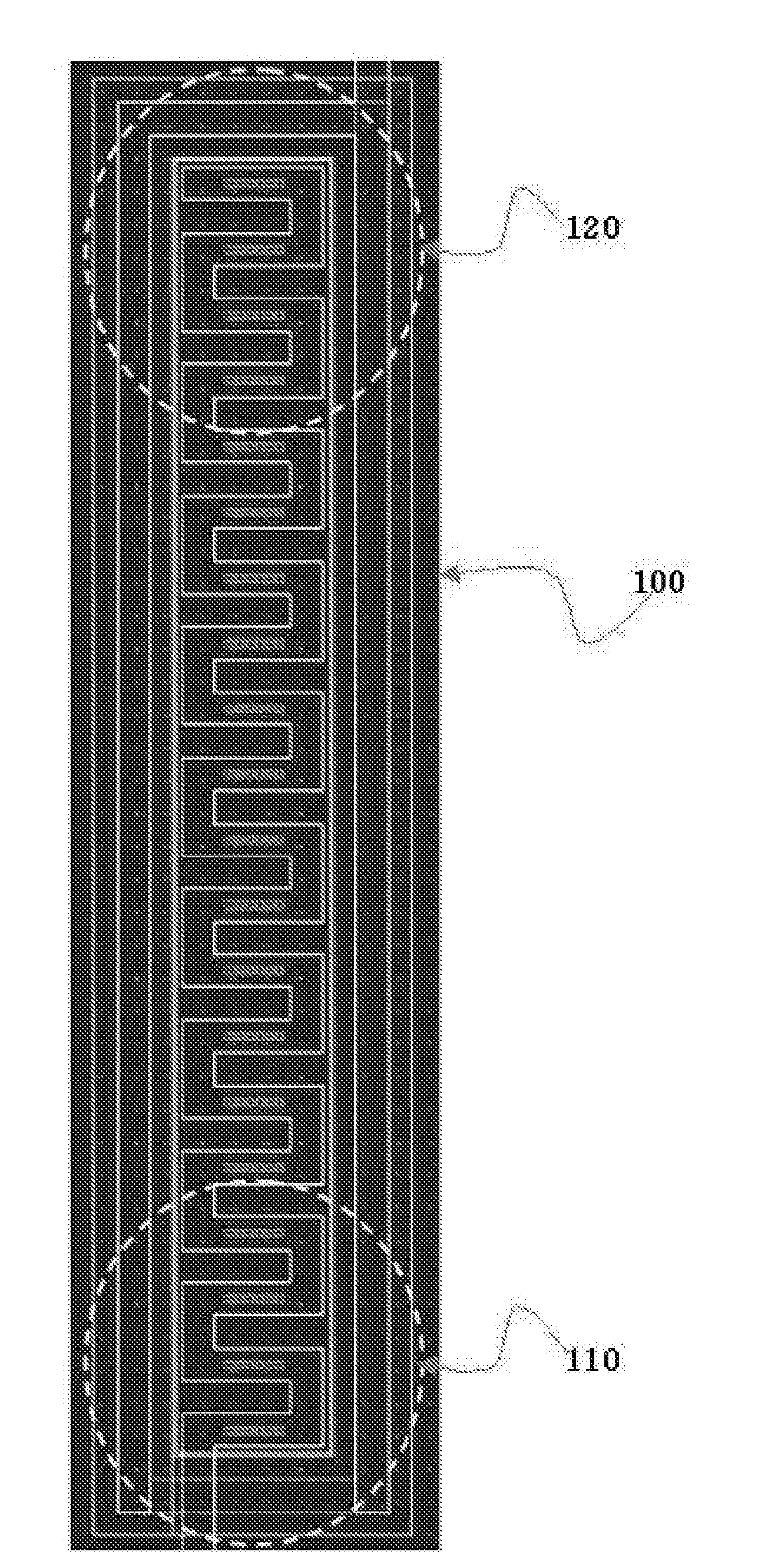
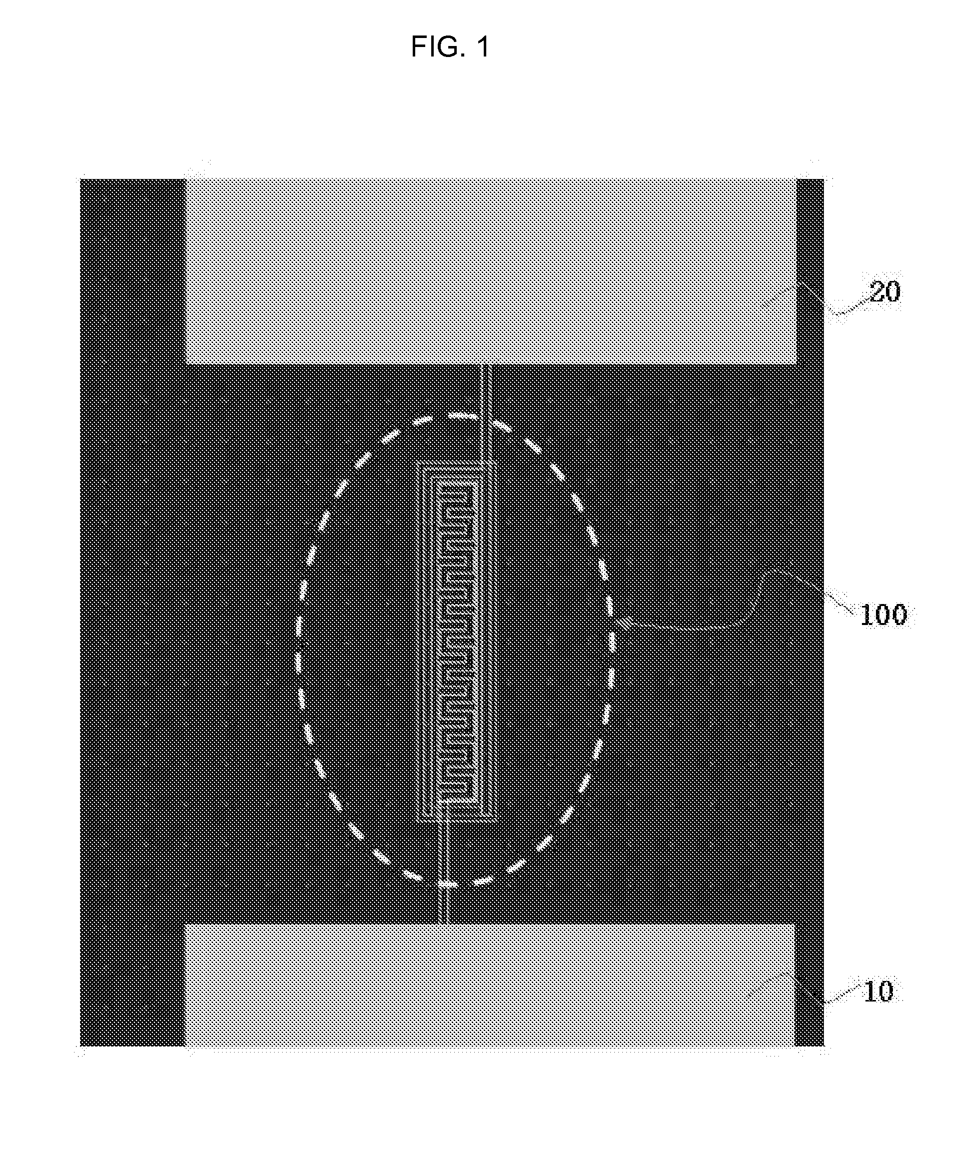
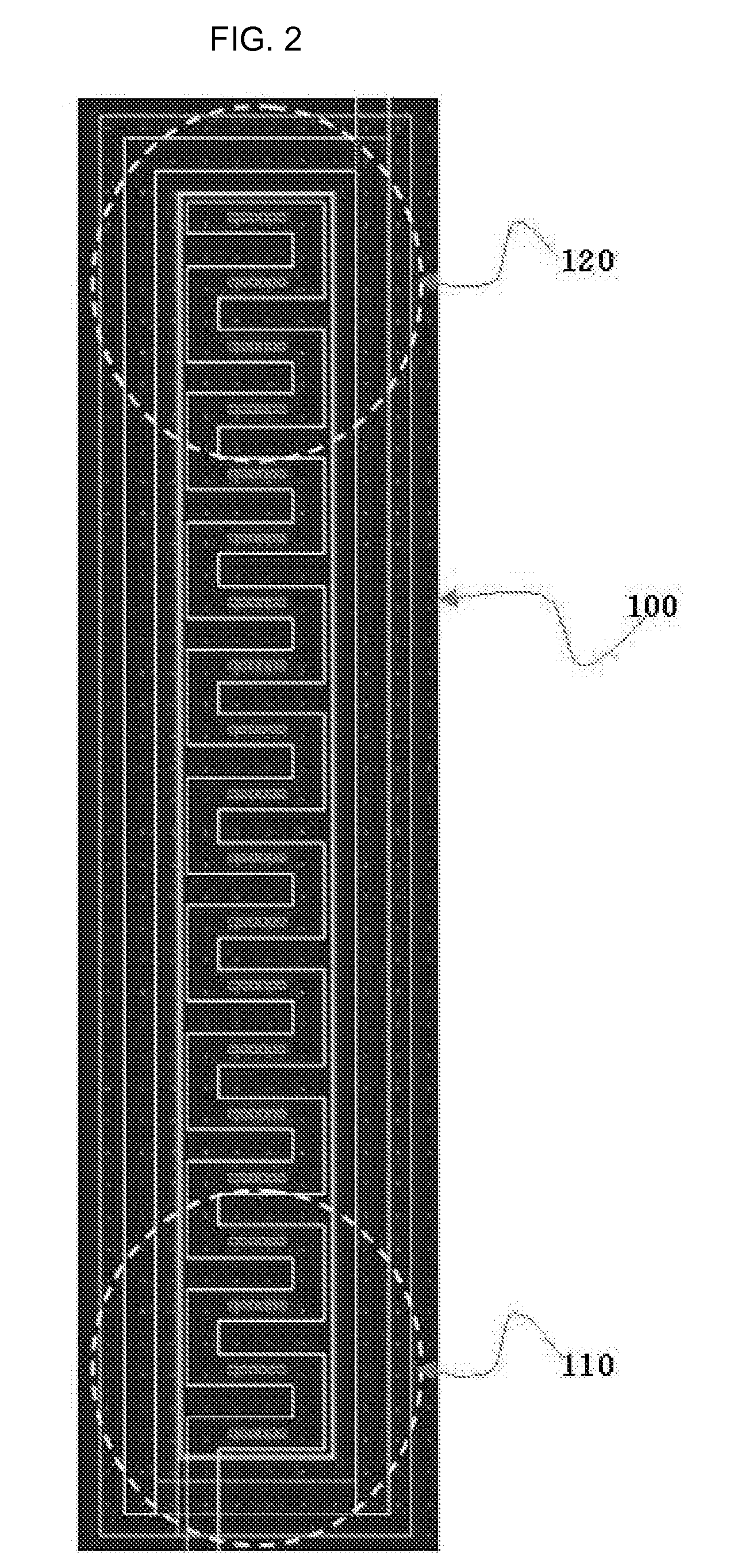
[0025]FIG. 1 is a layout of a TEG pattern according an embodiment of the present invention. FIG. 2 is an enlarged layout of the TEG pattern, and FIGS. 3 and 4 are each an enlarged layout showing a well pick-up area 120 and a metal strap area 110, respectively. FIG. 5 is an enlarged layout of a TEG pattern (C) in the well pick-up area 120 shown in FIG. 3, and FIG. 6 is a cross-sectional view taken along line PQ of the layout shown in FIG. 5.

[0026]As shown in FIGS. 1 and 2, the TEG pattern 100 according to a first embodiment comprises a well pick-up area 120 including a plurality of island type diode TEGs; a metal strap area 110 including the plurality of island type diode TEGs; a first or lower metal pad 10 applying a potential to the metal strap area 110; and a second or upper metal pad 20 detecting leakage current from the well pick-up area 120 as a result of the potential applied by the lower metal pad 10.

[0027]In particular, in manufacturing the semiconductor device, the present ...


PUM


Abstract

A TEG pattern comprises: a plurality of device isolation layer patterns having a predetermined gap; an active area pattern between adjacent device isolation layer patterns; and metal 1 contact patterns in the active region pattern.

Description

[0001]The present application claims priority under 35 U.S.C. 119 and 35 U.S.C. 365 to Korean Patent Application No. 10-2006-135771 (filed on Dec. 27, 2006), which is hereby incorporated by reference in its entirety.BACKGROUND[0002]1. Field of the Invention[0003]The invention relates to a TEG pattern (Test Element Group pattern) and a method for testing a semiconductor device using the same.[0004]2. Description of the Related Art[0005]In order to confirm whether the progressing results of the respective processes in a semiconductor manufacturing process are acceptable or preferable, the thickness, resistance, concentration, degree of contamination, critical dimensions, and electrical characteristics of devices or structures therein should be measured. In such a measurement process, the wafer of the semiconductor device may be damaged. As a result, one may be incapable of monitoring characteristics of an actual wafer in process (e.g., during the manufacturing process or between steps...

Claims


Application Information

Patent Timeline
Patent Type & Authority Applications(United States)
IPC IPC(8): G01R31/02H01L23/58
CPCG01R31/2648H01L22/34G01R31/2884H01L22/00
Inventor HONG, JI HO
Owner DONGBU HITEK CO LTD
Features
  • R&D
  • Intellectual Property
  • Life Sciences
  • Materials
  • Tech Scout
  • Unparalleled Data Quality
  • Higher Quality Content
  • 60% Fewer Hallucinations
Learn More