Pixel circuit, display, and method for driving pixel circuit

a pixel circuit and circuit technology, applied in the field of pixel circuits, display and method of driving pixel circuits, can solve the problems of large variation in luminance, adverse effects on light emission luminance, and difficulty in realizing large-size and high-definition displays, so as to reduce the area of the pixel array, enhance the simplification effect of the pixel circuit, and reduce the number of components and interconnections in the pixel circuit.

Active Publication Date: 2008-07-03
JOLED INC
View PDF2 Cites 80 Cited by
  • Summary
  • Abstract
  • Description
  • Claims
  • Application Information

AI Technical Summary

Benefits of technology

[0047]In particular, if the video signal line is used also as an interconnect for supplying the initialization potential to the sampling transistor and the initialization transistor and control is so implemented that the video signal of which potential is sequentially switched between the initialization potential and the signal potential is supplied to the sampling transistor and the initialization transistor, there is no need to provide a dedicated interconnect for the initialization potential, and therefore the effect of the pixel circuit simplification is enhanced.
[0048]That is, it is sufficient to add modification specific to the present invention based on the 2TR-drive configuration. Therefore, the numbers of components and interconnects in the pixel circuit can be reduced compared with the 5TR-drive configuration. This allows reduction in the area of the pixel array part, which makes it easy to achieve enhancement in the definition of a display. Thus, with a simplified pixel circuit, the function to correct luminance variation due to variations in characteristics of the elements can be realized.

Problems solved by technology

However, a display of the simple-matrix system involves e.g. a problem that it is difficult to realize a large-size and high-definition display although the configuration thereof is simple.
Therefore, in the case of the constant-voltage driving, even slight variation in the voltage and element characteristics causes large variation in the current, resulting in large variation in the luminance.
If there are such variation in characteristics of the drive active element and change in characteristics of the electro-optical element, the light emission luminance is adversely affected even in the constant-current driving system.
As a result, this scheme has a 5TR-drive configuration employing five transistors, including a drive transistor and sampling transistor, and hence the configuration of the pixel circuit is complicated.
Because the number of components in the pixel circuit is large, enhancement in the definition of the display is precluded.
As a result, it is difficult for the 5TR-drive configuration to be applied to a display used in a small electronic apparatus such as a portable apparatus (mobile apparatus).

Method used


Image

  • Pixel circuit, display, and method for driving pixel circuit
  • Pixel circuit, display, and method for driving pixel circuit
  • Pixel circuit, display, and method for driving pixel circuit

Examples


Embodiment Construction

[0071]An embodiment of the present invention will be described in detail below with reference to the accompanying drawings.

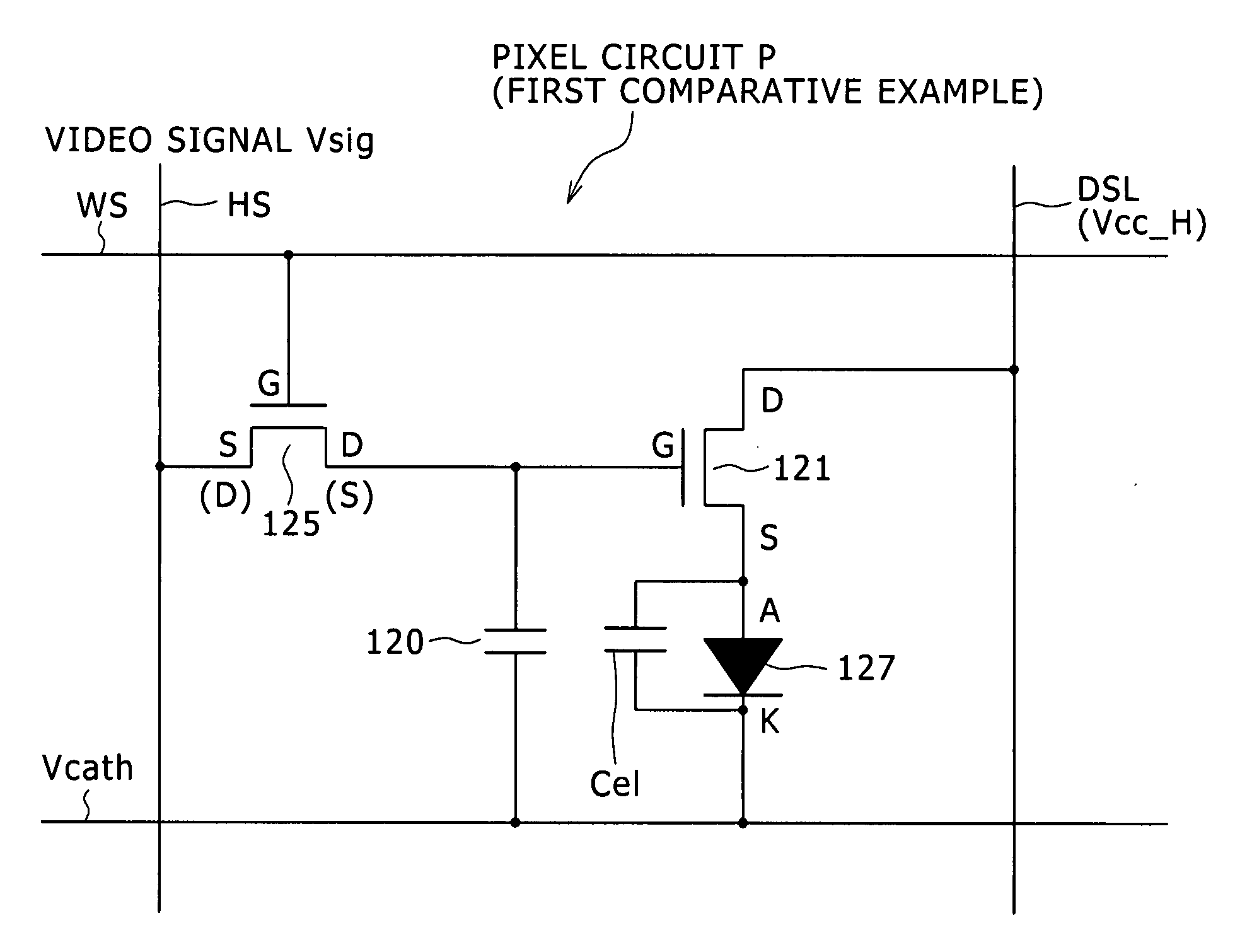
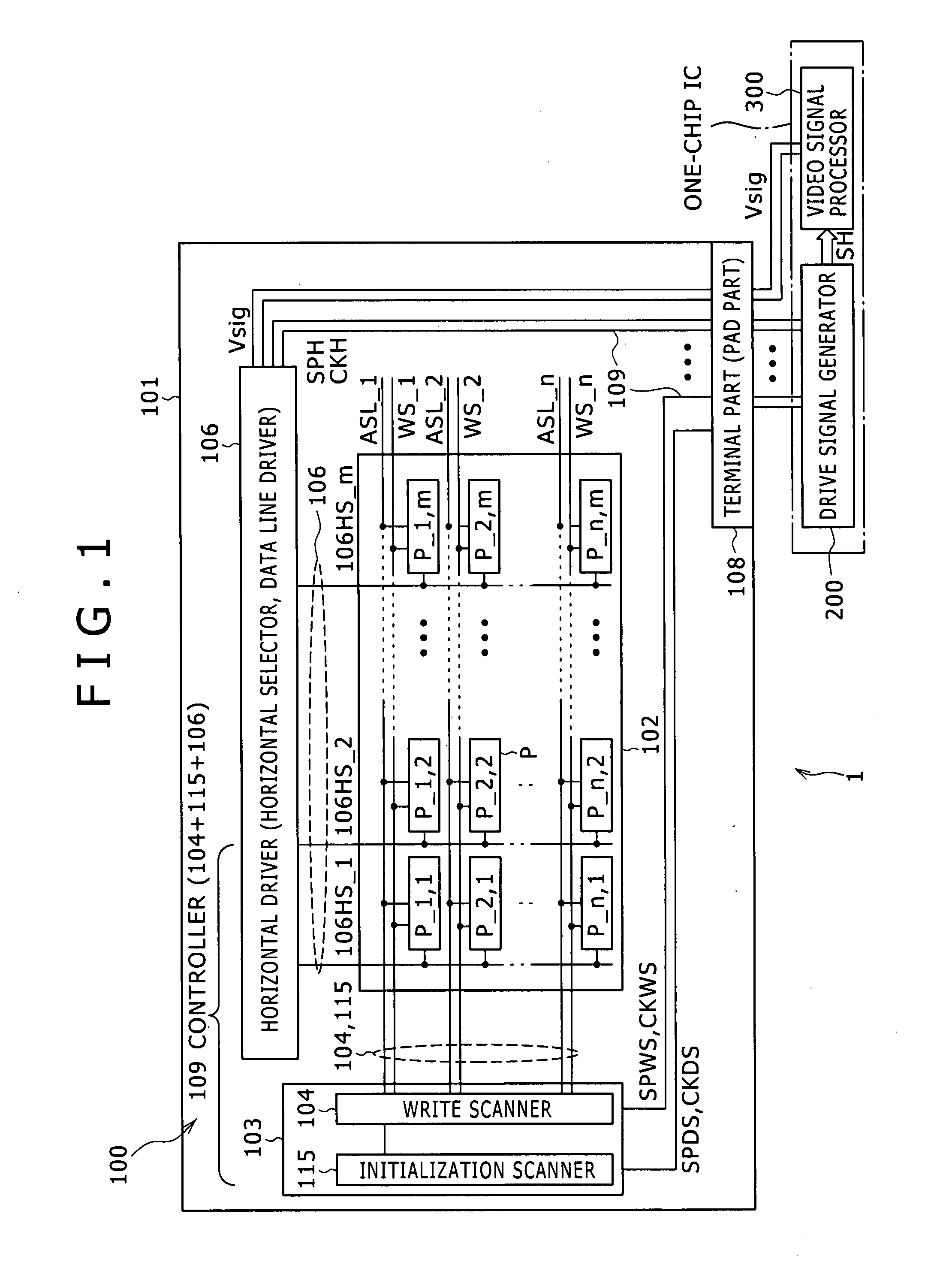
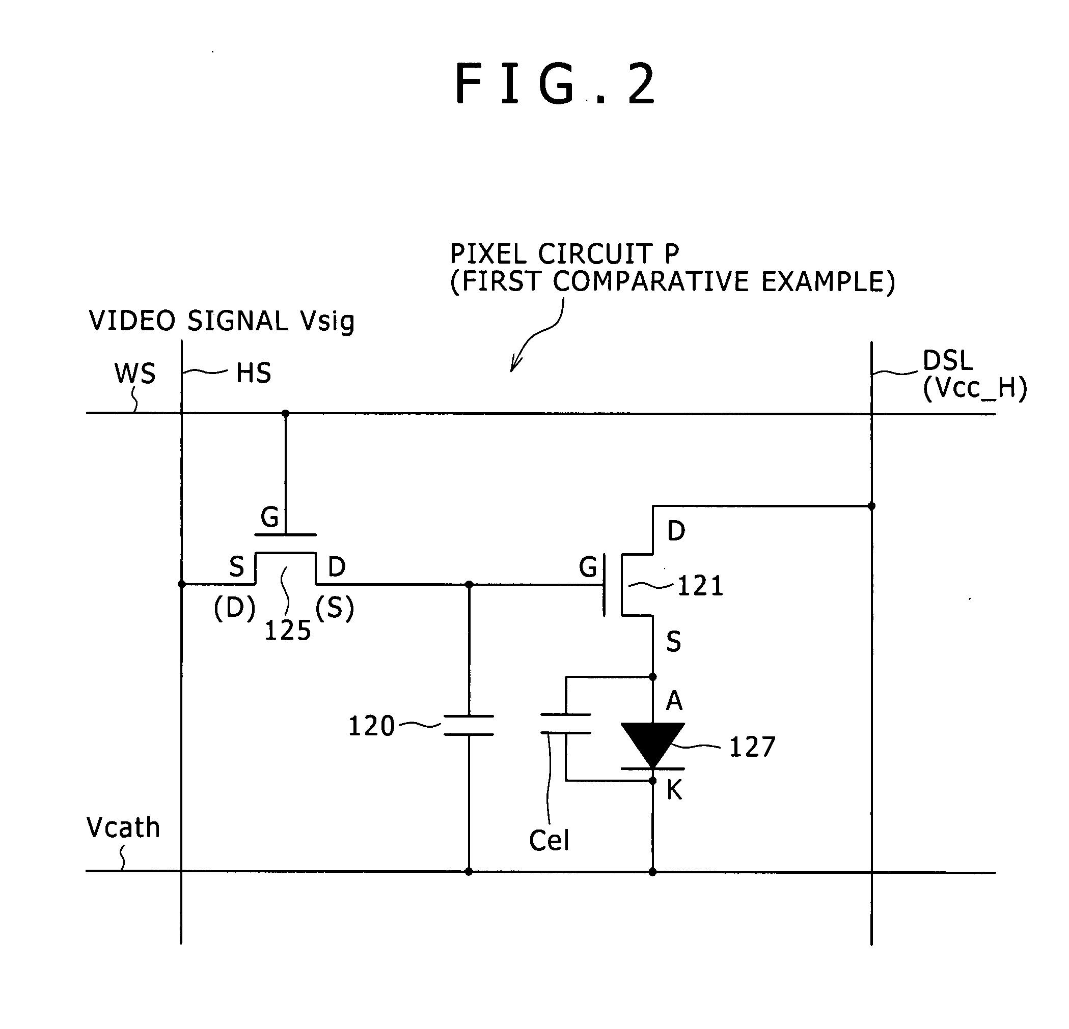
[0072]FIG. 1 is a block diagram schematically showing the configuration of an active-matrix display according to one embodiment of the present invention. The following description will deal with an example in which the present embodiment is applied to an active-matrix organic EL display (hereinafter, referred to as an “organic EL display”) obtained by forming organic EL elements as display elements (electro-optical elements, light-emitting elements) for pixels on a semiconductor substrate on which poly-silicon thin film transistors (TFTS) are formed as active elements.

[0073]The organic EL elements used as display elements for pixels in the following specific description are merely one example, and the display elements are not limited to the organic EL elements. All of the embodiment to be described below can be similarly applied to all of general display element...


PUM


Abstract

There is provided a display including: a pixel array part configured to include pixel circuits arranged in a matrix, each of the pixel circuits having a drive transistor, a holding capacitor, an electro-optical element, a sampling transistor, and an initialization transistor, a drive current based on information held in the holding capacitor being produced by the drive transistor and being applied to the electro-optical element for light emission of the electro-optical element; and a controller configured to include a write scanner, a horizontal driver, and an initialization scanner.

Description

CROSS REFERENCES TO RELATED APPLICATIONS[0001]The present invention contains subject matter related to Japanese Patent Application JP 2006-352560 filed in the Japan Patent Office on Dec. 27, 2006, the entire contents of which being incorporated herein by reference.BACKGROUND OF THE INVENTION[0002]1. Field of the Invention[0003]The present invention relates to a pixel circuit (referred to also as a pixel) including an electro-optical element (referred to also as a display element and a light-emitting element), a display having a pixel array part in which the pixel circuits are arranged in a matrix, and a method for driving the pixel circuit. More specifically, the invention relates to a pixel circuit having as a display element an electro-optical element of which luminance changes depending on the magnitude of a drive signal, an active-matrix display in which each pixel circuit has active elements and driving for displaying is carried out by the active elements on a pixel-by-pixel ba...

Claims


Application Information

Patent Timeline
Patent Type & Authority Applications(United States)
IPC IPC(8): G09G3/30
CPCG09G3/3233G09G3/3266G09G2320/045G09G2300/0842G09G2320/043G09G2300/0819G09G3/20G09G3/30G09G3/32H05B33/12
Inventor IIDA, YUKIHITOUCHINO, KATSUHIDE
Owner JOLED INC
Why Eureka
Try Eureka