Developing unit and image forming apparatus having the same

a technology of image forming apparatus and development unit, which is applied in the direction of electrographic process apparatus, instruments, optics, etc., can solve the problems of image defects, increase in the number of components and manufacturing costs, and the surface of the respective photosensitive member may not be charged uniformly, so as to reduce the surface potential of the photosensitive member, reduce the number of components and the effect of the manufacturing cost of the image forming apparatus

Inactive Publication Date: 2008-07-03
S PRINTING SOLUTION CO LTD
View PDF7 Cites 44 Cited by
  • Summary
  • Abstract
  • Description
  • Claims
  • Application Information

AI Technical Summary

Benefits of technology

[0013]Therefore, aspects of the invention relate to providing an image forming apparatus that is equipped with a lamp capable of resetting a surface potential and decreasing a surface potential of a photosensitive member, thereby reducing a number of components and manufacturing costs of an image forming apparatus.

Problems solved by technology

However, because of a residual electric potential on the photosensitive members after the transfer, the surface of the respective photosensitive members may not be charged uniformly.
This residual electric potential affects the formation of a successive electrostatic latent image and causes image defects, such as a ghost images.
However, the installation of the eraser lamp and the pre-transfer lamp in the conventional image forming apparatus causes an increase in the number of components and in the manufacturing costs.

Method used


Image

  • Developing unit and image forming apparatus having the same
  • Developing unit and image forming apparatus having the same
  • Developing unit and image forming apparatus having the same

Examples


Embodiment Construction

[0027]Reference will now be made in detail to exemplary embodiments of the present invention, examples of which are illustrated in the accompanying drawings, wherein like reference numerals refer to like elements throughout. The embodiments are described below to explain the present invention, by referring to the figures.

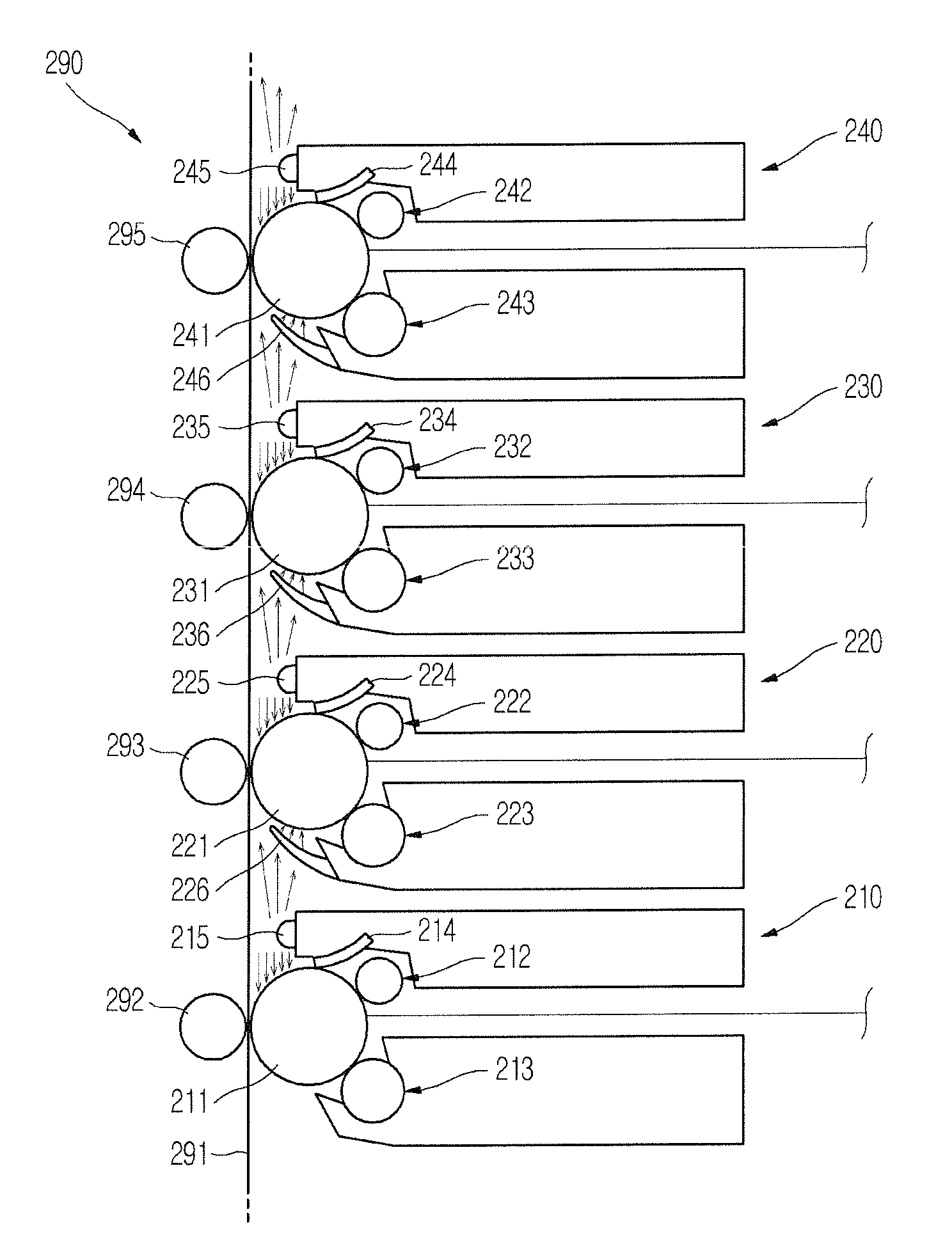
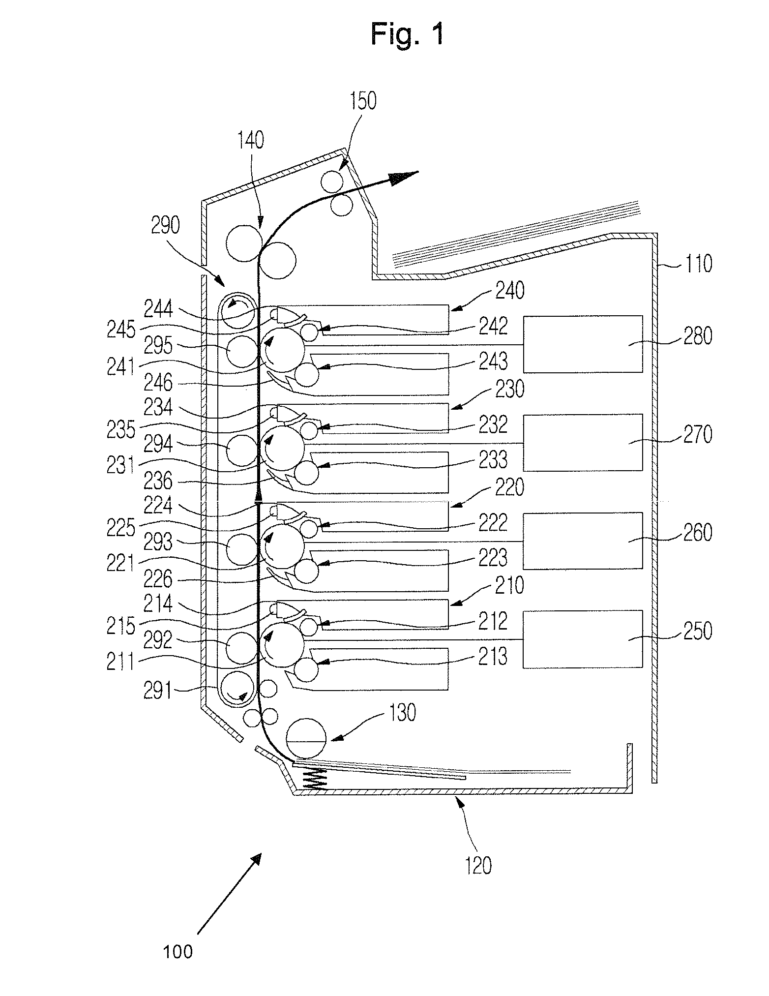
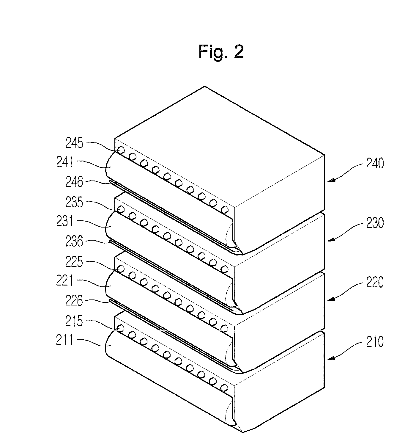
[0028]As shown in FIG. 1, an image forming apparatus 100, according to aspects of the present invention, includes: a main body 110 to house various components and form an external appearance; a plurality of developing units 210, 220, 230, and 240 to form visible images of different colors; a plurality of exposure units 250, 260, 270, and 280 mounted to the respective developing units 210, 220, 230, and 240, to irradiate a corresponding light beam onto the corresponding developing units 210, 220, 230, and 240, according to an image signal; and a transfer unit 290 to transfers the visible images from the respective developing units 210, 220, 230, and 240 onto a printi...


PUM


Abstract

An image forming apparatus including: a plurality of photosensitive members on which electrostatic latent images are formed; a plurality of charge units to charge the respective photosensitive members with an electric potential; at least one exposure unit which irradiates light to the respective photosensitive members; a plurality of developer supply devices, which adhere a developer to the respective photosensitive members, to form visible images on a surface of the respective photosensitive members; a transfer unit, which transfers the visible images formed on the respective photosensitive members to a transfer medium; and a plurality of exposure lamps which are mounted between the plurality of photosensitive members. Each of the exposure lamps radiates light to the surface of one of two adjacent photosensitive members, after completion of the transfer, to reset a surface potential thereof, and irradiates light to the surface of the other photosensitive member, on which the visible image is formed, to decrease a surface potential thereof.

Description

CROSS-REFERENCE TO RELATED APPLICATION[0001]This application claims the benefit of Korean Application No. 2007-679, filed Jan. 3, 2007, in the Korean Intellectual Property Office, the disclosure of which is incorporated herein by reference.BACKGROUND[0002]1. Field of the Invention[0003]Aspects of the present invention relate to an image forming apparatus.[0004]2. Description of the Related Art[0005]Generally, an electrophotographic image forming apparatus is configured such that a light beam is radiated onto a photosensitive member charged with an electric potential, to form an electrostatic latent image on the surface of the photosensitive member. The electrostatic latent image is developed into a visible image, by adhering toner to the electrostatic latent image, and the visible image is transferred and fixed onto a printing medium. The electrophotographic image forming apparatus can be classified as a mono-image forming apparatus, if it can print only a black and white image, or ...

Claims


Application Information

Patent Timeline
Patent Type & Authority Applications(United States)
IPC IPC(8): G03G21/00
CPCG03G15/169G03G2215/0119G03G21/08G03G15/00
Inventor JUNG, HYUN SUNKIM, JIN CHEOLYANG, YOO SEOK
Owner S PRINTING SOLUTION CO LTD
Why Eureka
Try Eureka