Process gas introducing mechanism and plasma processing device

a technology of plasma processing device and introducing mechanism, which is applied in the direction of electric discharge tube, chemical vapor deposition coating, coating, etc., can solve the problems of increasing maintenance time, lowering device operation rate, lowering semiconductor device production yield, etc., and improving the in-surface uniformity of the substrate. , the effect of lowering the in-surface uniformity

Inactive Publication Date: 2006-03-23
TOKYO ELECTRON LTD
View PDF7 Cites 43 Cited by
  • Summary
  • Abstract
  • Description
  • Claims
  • Application Information

AI Technical Summary

Benefits of technology

[0032] The sixth aspect of the present invention is to resolve such a problem that, in the conventional susceptor, an area for supporting the wafer is cut to have a recess portion and an impedance in the outer periphery of the recess portion gets larger than that of the central portion thereof, so that a bias for producing a plasma and the like may be affected, and thus, lowering the in-surface uniformity in the plasma processing. Further, in the mask of the mounting table where the substrate t...

Problems solved by technology

As a result, such problems as lowering in an operation rate of the device, lowering in a production yield of a semiconductor device and the like, are incurred.
However, when replacing the cover shield 411, the bell jar 401, the gas introducing ring 408 and the lid base 407 need to be detached, thereby increasing the time for maintenance, which becomes problematic.
Further, the gas introducing ring 408 has a complicated configuration wherein the gas channel 408b and the like are formed, and cost of a compon...

Method used


Image

  • Process gas introducing mechanism and plasma processing device
  • Process gas introducing mechanism and plasma processing device
  • Process gas introducing mechanism and plasma processing device

Examples


first embodiment

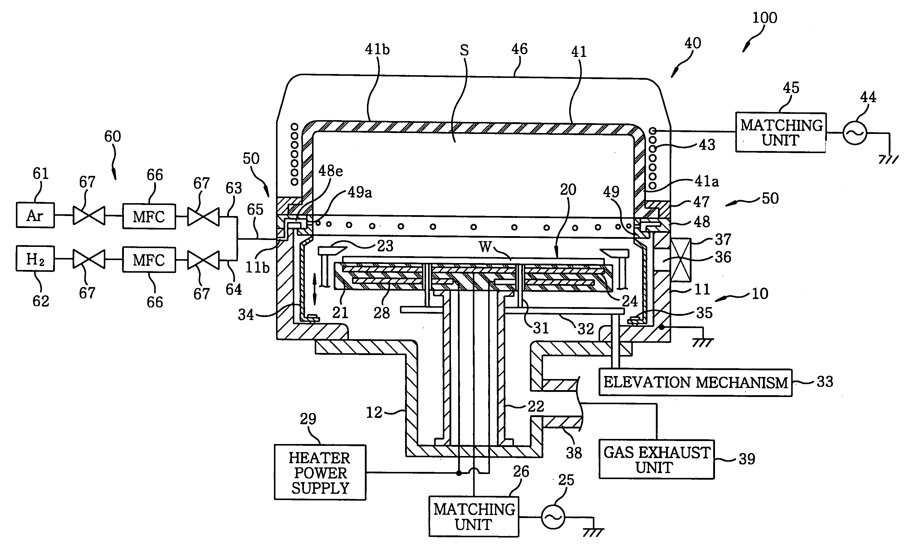
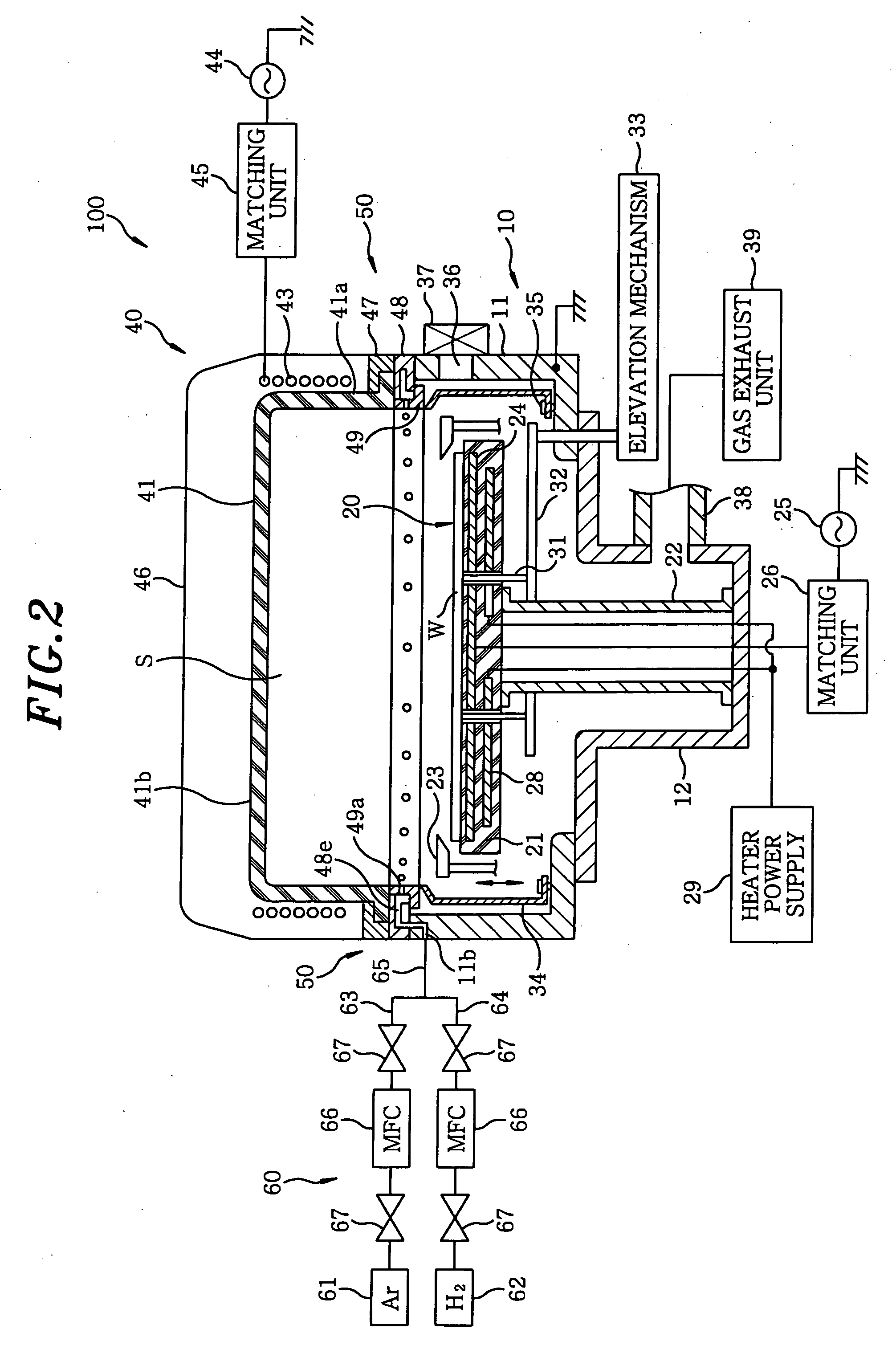
[0054]FIG. 2 is a schematic configuration of a plasma processing apparatus in accordance with a first embodiment of the present invention. A plasma processing apparatus 100 for performing a plasma processing on a substrate to be processed is employed, e.g., in a processing for plasma-etching to remove an impurity layer containing an oxide film such as a native oxide or the like, which is formed on a metal film or a silicon formed on the substrate to be processed.

[0055] The plasma processing apparatus 100 includes a chamber 10 accommodating therein a semiconductor wafer as a substrate to be processed; a wafer supporting portion 20 supporting the semiconductor wafer in the chamber 10; a plasma generation unit 40, installed to cover the chamber 10, for generating a plasma in a processing space S where a plasma processing is performed on the wafer; a gas introducing mechanism 50 for introducing a gas for producing a plasma into the processing space S; and a gas supply unit 60 for suppl...

second embodiment

[0102] In the following, a second embodiment of the present invention will be discussed.

[0103]FIG. 9 is a schematic view of a configuration of a plasma processing apparatus in accordance with the second embodiment of the present invention. The plasma processing apparatus 100′, like as the plasma processing apparatus 100 of the first embodiment, is applied to a process for plasma-etching to remove an impurity layer containing an oxide film, e.g., a native oxide film or the like, formed on a metal film or a silicon formed on a substrate to be processed. Further, the plasma processing apparatus 100′ has a chamber 10′ accommodating therein a semiconductor wafer as a substrate to be processed; a wafer supporting portion 20′ supporting the semiconductor wafer inside the chamber 10′; a plasma generation unit 40′, installed to cover the chamber 10′, for producing a plasma in a processing space S where a plasma processing is performed on a wafer; a gas introducing mechanism 50′ introducing ...

third embodiment

[0139] In the following, a third embodiment of the present invention will be explained. The third embodiment is characterized by a mounting configuration of the semiconductor wafer W as a substrate to be processed.

[0140]FIG. 13 is a schematic cross sectional view showing a mounting configuration of the semiconductor wafer in the plasma processing apparatus in accordance with the third embodiment of the present invention. In the present embodiment, a cap shaped mask plate 170 is provided on a susceptor 21 attachably and detachably to form a wafer supporting portion 20″; and the wafer W is configured to be mounted on a surface of the mask plate 170. Since the mounting configuration of the semiconductor wafer or configurations around the chamber are the same as in the second embodiment, identical reference numerals in FIG. 13 will be used for the corresponding parts having substantially same functions and configurations of FIG. 10 in the second embodiment, and explanations thereof wil...


PUM

PropertyMeasurementUnit
Dielectric polarization enthalpyaaaaaaaaaa
Flow rateaaaaaaaaaa
Diameteraaaaaaaaaa

Abstract

A processing gas introducing mechanism for introducing a processing gas into a processing space is provided between a plasma generation unit and a chamber of a plasma processing apparatus. The processing gas introducing mechanism includes a gas introducing base having therein a gas introducing path for introducing the processing gas into the processing space, and a near ring-shaped gas introducing plate equipped in the hole part of the gas introducing base such that it can be detached therefrom. Herein, the gas introducing base has a hole part forming one portion of the processing space in a central portion thereof, and the gas introducing plate has plural gas discharge holes communicating with the processing space to discharge thereinto the processing gas from the gas introducing path.

Description

This application is a Continuation Application of PCT International Application No. PCT / JP04 / 006165 filed on Apr. 28, 2004, which designated the United States.FIELD OF THE INVENTION [0001] The present invention relates to a processing gas introducing mechanism for introducing a processing gas for use in a substrate processing, and a plasma processing apparatus for performing a plasma processing on a substrate by introducing a processing gas. BACKGROUND OF THE INVENTION [0002] In a semiconductor manufacturing processing, e.g., a Ti film is formed on a bottom portion of a contact hole formed in a silicon wafer as an object to be processed; a TiSi is formed by an interdiffusion between Ti and Si of a substrate; a barrier layer such as a TiN or the like is formed on the TiSi; an Al layer, a W layer, a Cu layer and the like are formed on the barrier layer; and thus, holes are filled and wirings are fabricated. Conventionally, for performing a series of processings as described above, the...

Claims


Application Information

Patent Timeline
IPC IPC(8): H01L21/306C23C16/00H01J37/32H01L21/00H01L21/3065
CPCH01J37/3244H01J37/32449H01L21/67126H01L21/67103H01L21/67069H01L21/68742H01L21/68H01J37/3211
Inventor KAMAISHI, TAKAYUKISHIMAMURA, AKINORIMORISHIMA, MASATO
Owner TOKYO ELECTRON LTD
Why Eureka
Try Eureka