Metal core solder ball interconnector fan-out wafer level package and manufacturing method therefor

Active Publication Date: 2018-12-13
HANA MICRON
View PDF10 Cites 13 Cited by
  • Summary
  • Abstract
  • Description
  • Claims
  • Application Information

AI Technical Summary

Benefits of technology

[0032]When the interconnector is formed using the metal-core solder ball, a size of a ball can be minimized, and a height of the interconnec

Problems solved by technology

Since the via plug is formed of a metal, there is a limitation in that stress caused by a difference in coefficient of thermal expansion (CTE) between molding compounds adjacent to the via plug cannot be resolved.
However, since additional deposition and etching processes are required to form a liner including a metal layer and/or a dielectric layer, the number of processes greatly increases and costs also increase.
In addition, since a carrier i

Method used


Image

  • Metal core solder ball interconnector fan-out wafer level package and manufacturing method therefor
  • Metal core solder ball interconnector fan-out wafer level package and manufacturing method therefor
  • Metal core solder ball interconnector fan-out wafer level package and manufacturing method therefor

Examples


Example

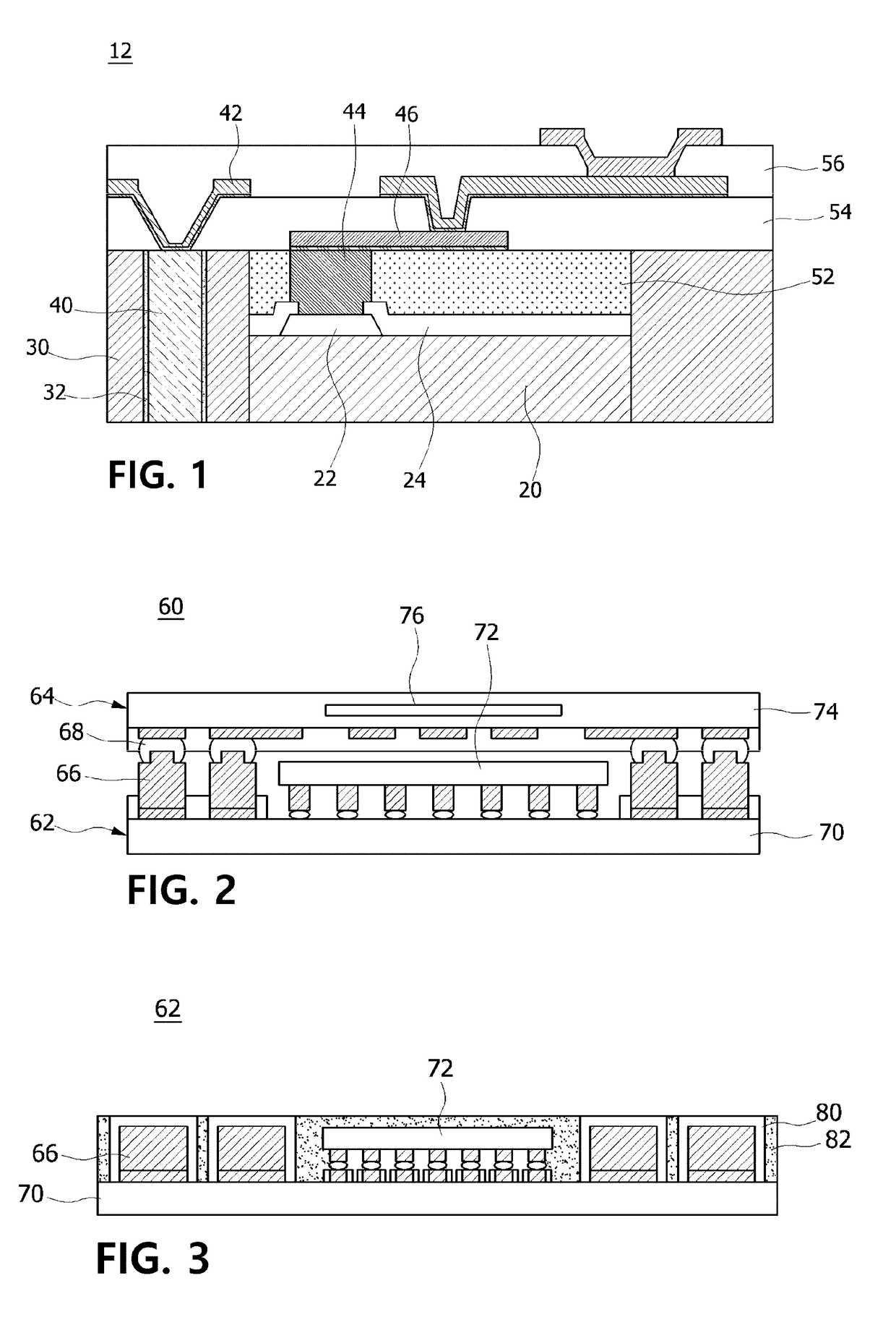
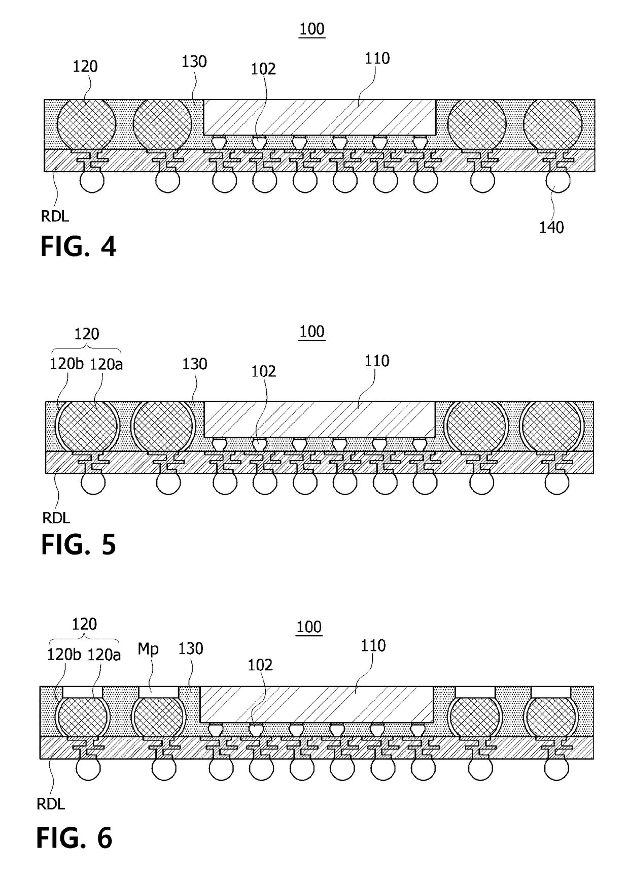
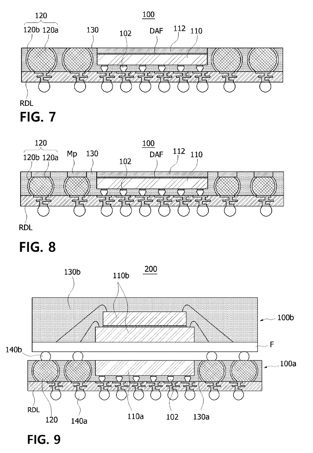
[0045]Advantages and features of the present invention and methods of achieving the same will be clearly understood with reference to the following detailed embodiments. The present invention may, however, be embodied in many different forms and should not be construed as limited to the embodiments set forth herein. Rather, the embodiments are provided so that this disclosure will be thorough and complete, and will fully convey the scope of the present invention to those skilled in the art. The scope of the present invention is defined by the appended claims. In the drawings, the size and relative sizes of layers and regions may be exaggerated for clarity. Like numbers refer to like elements throughout the specification.

[0046]Furthermore, the embodiments of the present invention are described herein with reference to plan and / or cross-section illustrations that are schematic illustrations of the idealized embodiments of the present invention. Accordingly, for example, shapes of illu...


PUM


Abstract

fan-out wafer level package is disclosed, which comprises: a redistribution layer; a semiconductor chip electrically connected with the redistribution layer through a bump; a protective member protecting the semiconductor chip, wherein a part of the protective member is removed such that the upper surface of the semiconductor chip is exposed in order to dissipate heat and prevent warpage; and an interconnector disposed outside the semiconductor chip at substantially the same level and having a lower part electrically connected with the redistribution layer and an upper part not being covered with the protective member, wherein the interconnector includes a metal core solder ball, the metal core solder ball includes a metal core and a solder buffer between the metal core and the protective member, and the metal core is formed of a combination of copper (Cu), nickel (Ni), and silver (Ag).

Description

FIELD OF THE DISCLOSURE[0001]The present invention relates to a fan-out wafer-level package, in which may upper and lower packages are connected using a copper (Cu) or another metal core solder ball type interconnector, to be used for a fan-out package-on-package (PoP), and a method of manufacturing the same. The present invention relates to a fan-out wafer-level package (C2FO-WLP) structure, which provides an interconnector using a metal-core solder ball of which a shape may be easily implemented and changed and appropriately adjusted to a fine pitch by adjusting a diameter of a ball. To suppress stress between a metal core and a mold, the C2FO-WLP structure minimizes stress due to a difference in coefficient of thermal expansion (CTE) between a metal and the mold and, at the same time, prevents oxidation of the metal by the metal core coated with a solder. In addition, the present invention relates to a method of manufacturing a C2FO-WLP, which is effective in dissipating heat of ...

Claims


Application Information

Patent Timeline
IPC IPC(8): H01L23/498H01L23/31H01L23/00H01L21/48H01L25/10
CPCH01L23/49866H01L24/16H01L21/4853H01L25/105H01L2224/16227H01L2924/1816H01L2225/1058H01L23/49816H01L23/3185H01L2224/04105H01L2224/12105H01L21/568H01L24/19H01L2224/32245H01L2224/73267H01L2224/92244H01L2924/18162H01L23/5389H01L23/49827H01L23/3128H01L21/6835H01L2221/68359H01L24/20H01L2224/73253H01L2224/94H01L2224/27436H01L2224/83191H01L2224/81191H01L2224/83005H01L2224/18H01L2224/32145H01L2224/48227H01L25/0657H01L2225/0651H01L25/50H01L2224/1134H01L2924/00014H01L2224/27H01L2924/0001H01L23/28H01L23/488H01L23/00H01L2224/13583H01L25/07H01L2224/13575H01L2224/13582H01L2224/13584H01L2224/1357H01L2224/13578H01L2224/1358H01L2224/13576
Inventor LEE, HYUN WOOJEONG, JIN WOOKKIM, HYUN JOOOCK, JIN YOUNG
Owner HANA MICRON
Why Eureka
Try Eureka