
Magnetic Random Access Memory Cells Having Split Subdigit Lines Having Cladding Layers Thereon and Methods of Fabricating the Same

a random access and memory cell technology, applied in the field of magnetic random access memory cells, can solve the problems of difficult generation of magnetic fields, limitation in improving the writing efficiency of mram cells, and difficulty in shrinking conventional mram cells

Inactive Publication Date: 2008-07-03
SAMSUNG ELECTRONICS CO LTD
View PDF6 Cites 10 Cited by
  • Summary
  • Abstract
  • Description
  • Claims
  • Application Information

AI Technical Summary

Benefits of technology

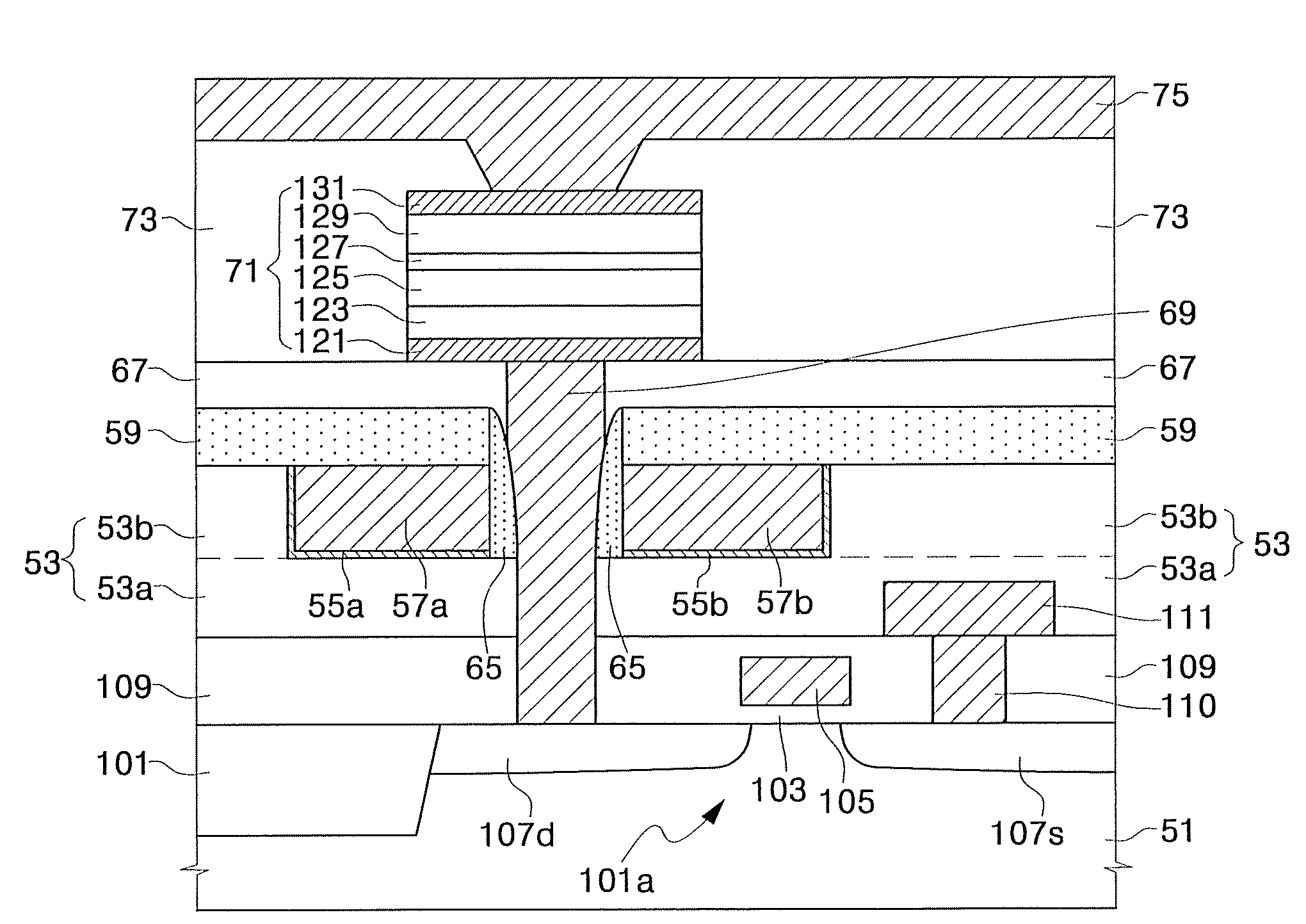
The present invention provides MRAM cells with split digit lines and methods of fabricating them. The MRAM cells have first and second sub-digit lines that are surrounded by first and second cladding layers. A magnetic resistor contact plug penetrates the first and second sub-digit lines and is electrically connected to a magnetic resistor. The MRAM cells have improved performance and stability. The methods of fabricating the MRAM cells involve forming a groove in an interlayer insulating layer and sequentially adding a conformal cladding layer and a bit line to the groove. A capping layer and insulating spacer are formed on the inner sidewalls of the groove. The MRAM cells have reduced chip area and improved performance.

Problems solved by technology

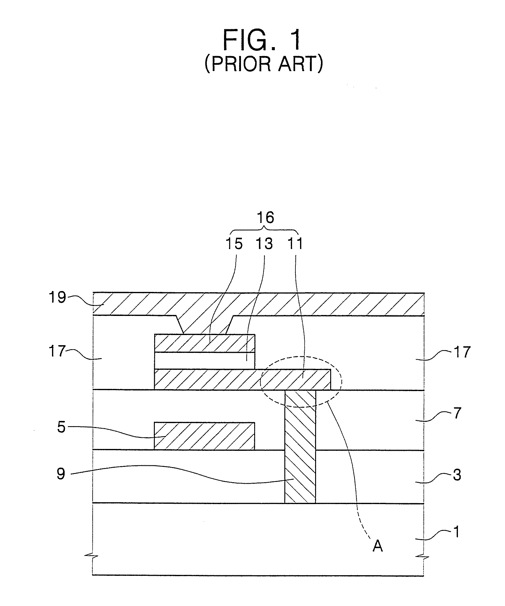
As a result, the extension A of the lower electrode 11 makes it difficult to shrink the conventional MRAM cell shown in FIG. 1.
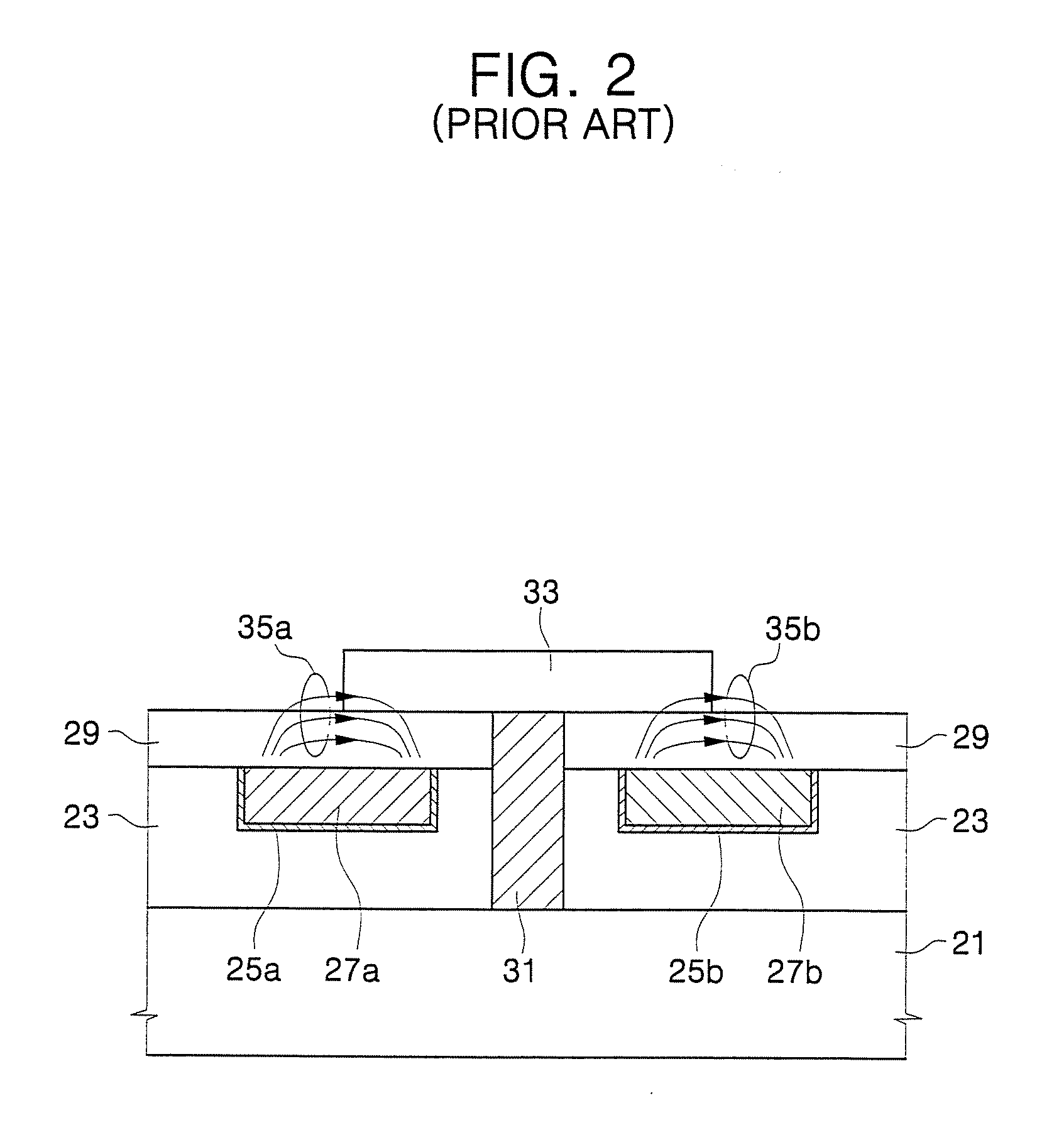
In other words, it may be difficult to generate a magnetic field that is uniformly distributed throughout the MTJ 33 during the writing operation.
Thus, there is a limitation in improving the writing efficiency of the MRAM cell, even though the MRAM cell having the split sub-digit lines 27a and 27b employs the cladding layers that concentrate the magnetic fields.

Method used


Image

  • Magnetic Random Access Memory Cells Having Split Subdigit Lines Having Cladding Layers Thereon and Methods of Fabricating the Same
  • Magnetic Random Access Memory Cells Having Split Subdigit Lines Having Cladding Layers Thereon and Methods of Fabricating the Same
  • Magnetic Random Access Memory Cells Having Split Subdigit Lines Having Cladding Layers Thereon and Methods of Fabricating the Same

Examples


Embodiment Construction

[0035]The present invention now will be described more fully hereinafter with reference to the accompanying drawings, in which embodiments of the invention are shown. However, this invention should not be construed as limited to the embodiments set forth herein. Rather, these embodiments are provided so that this disclosure will be thorough and complete, and will fully convey the scope of the invention to those skilled in the art. In the drawings, the thickness of layers and regions are exaggerated for clarity. Like numbers refer to like elements throughout. As used herein the term “and / or” includes any and all combinations of one or more of the associated listed items.

[0036]The terminology used herein is for the purpose of describing particular embodiments only and is not intended to be limiting of the invention. As used herein, the singular forms “a”, “an” and “the” are intended to include the plural forms as well, unless the context clearly indicates otherwise. It will be further...


PUM


Abstract

Magnetic RAM cells have split sub-digit lines surrounded by cladding layers and methods of fabricating the same are provided. The magnetic RAM cells include first and second sub-digit lines formed over a semiconductor substrate. Only a bottom surface and an outer sidewall of the first sub-digit line are covered with a first cladding layer pattern. In addition, only a bottom surface and an outer sidewall of the second sub-digit line are covered with a second cladding layer pattern. The outer sidewall of the first sub-digit line is located distal from the second sub-digit line and the outer sidewall of the second sub-digit line is located distal the first sub-digit line. Methods of fabricating the magnetic RAM cells are also provided.

Description

CROSS-REFERENCE TO RELATED APPLICATION[0001]This application is a divisional of application Ser. No. 11 / 077,669, filed Mar. 11, 2005 and claims the benefit of Korean Patent Application Nos. 2004-0019007 and 2004-0064030, filed Mar. 19, 2004 and Aug. 13, 2004 respectively, the contents of which are hereby incorporated herein by reference in their entirety.BACKGROUND OF THE INVENTION[0002]The present invention relates to semiconductor memory cells and methods of fabricating the same and, more particularly, to magnetic random access memory cells and methods of fabricating the same.[0003]Magnetic random access memory (MRAM) devices have been widely used as non-volatile memory devices, which can be operated at a low voltage and / or a high speed. In a unit cell of the MRAM devices, one bit of data is stored in a magnetic tunnel junction (MTJ) of a magnetic resistor. The MTJ generally includes first and second ferromagnetic layers and a tunneling insulation layer interposed between the firs...

Claims


Application Information

Patent Timeline
Patent Type & Authority Applications(United States)
IPC IPC(8): H01L43/12H01L21/00H01L21/8246H01L27/22H01L29/82H10N50/01H10N50/10
CPCB82Y10/00H01L43/12H01L43/08H01L27/228H10B61/22H10N50/01H10N50/10
Inventor PARK, JAE-HYUNKIM, HYEONG-JUNJEONG, WON-CHEOLJEONG, CHANG-WOOKJEONG, HONG-SIKJEONG, GI-TAE
Owner SAMSUNG ELECTRONICS CO LTD
Learn More