Power semiconductor device
- Summary
- Abstract
- Description
- Claims
- Application Information
AI Technical Summary
Benefits of technology
Problems solved by technology
Method used
Image

Examples
Embodiment Construction
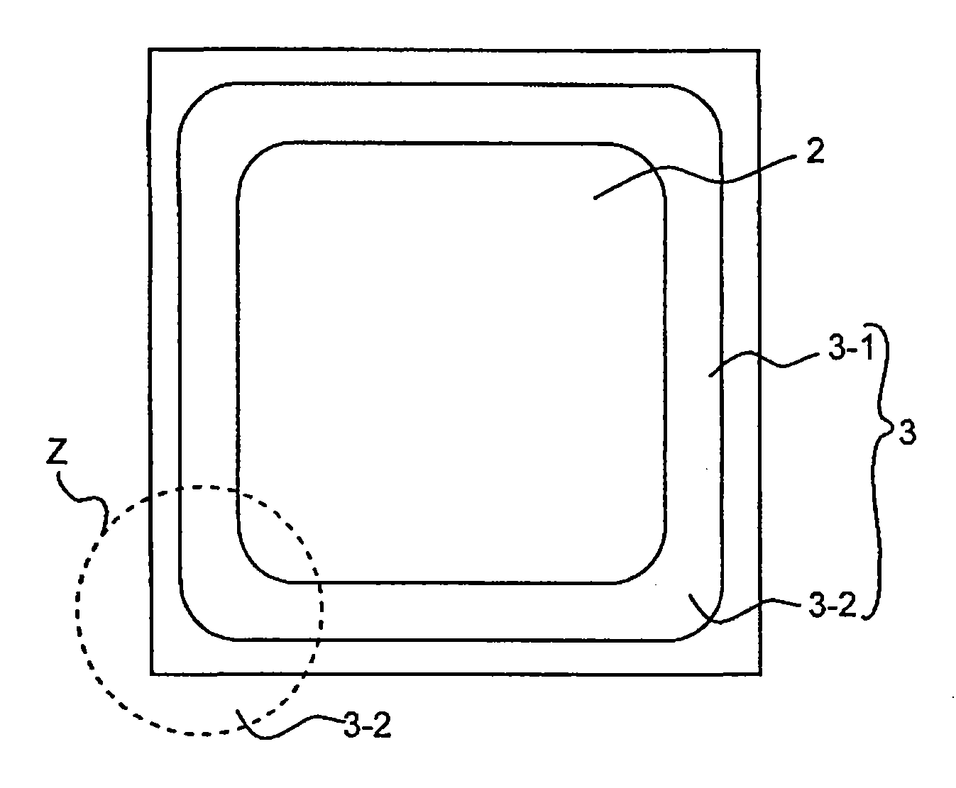
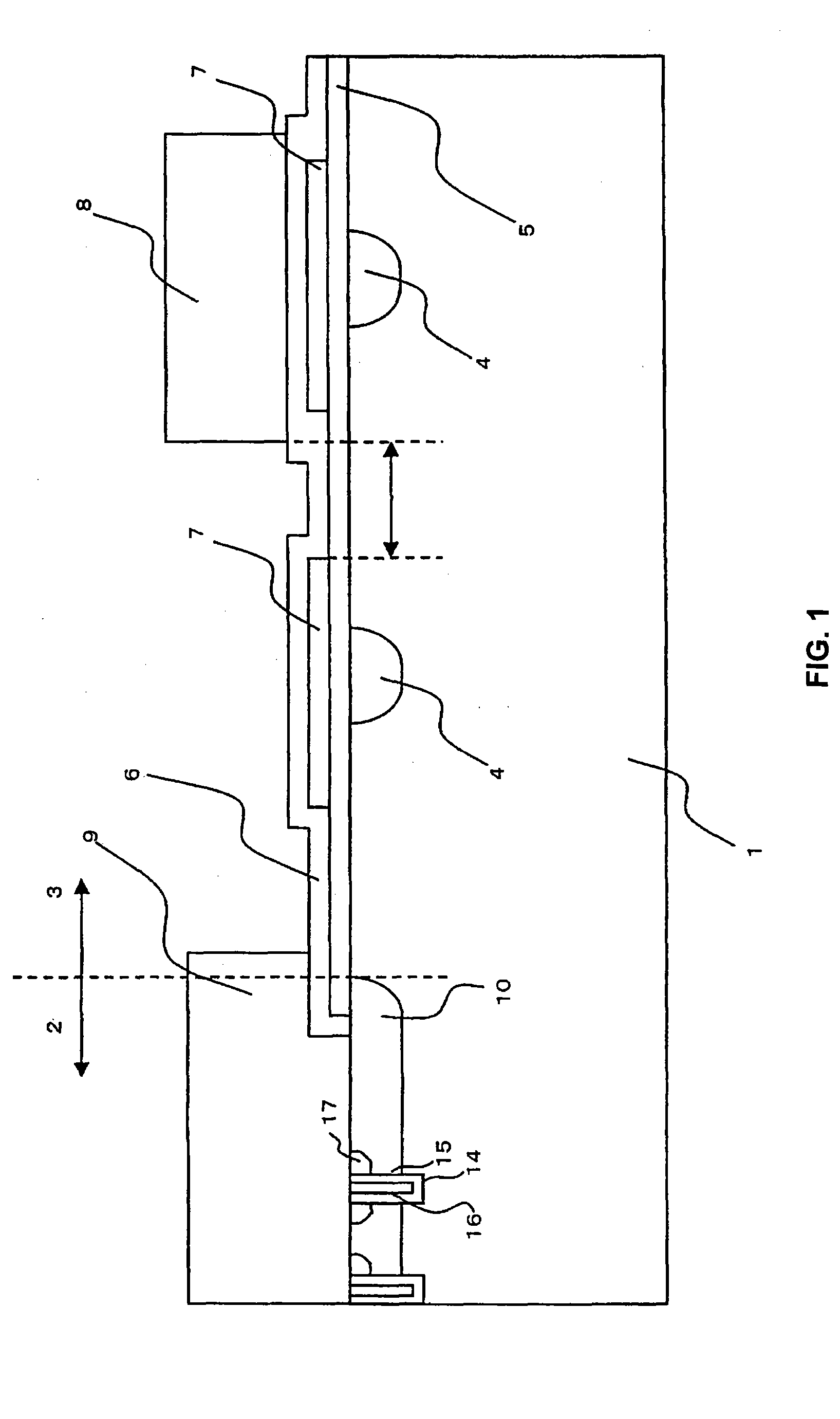
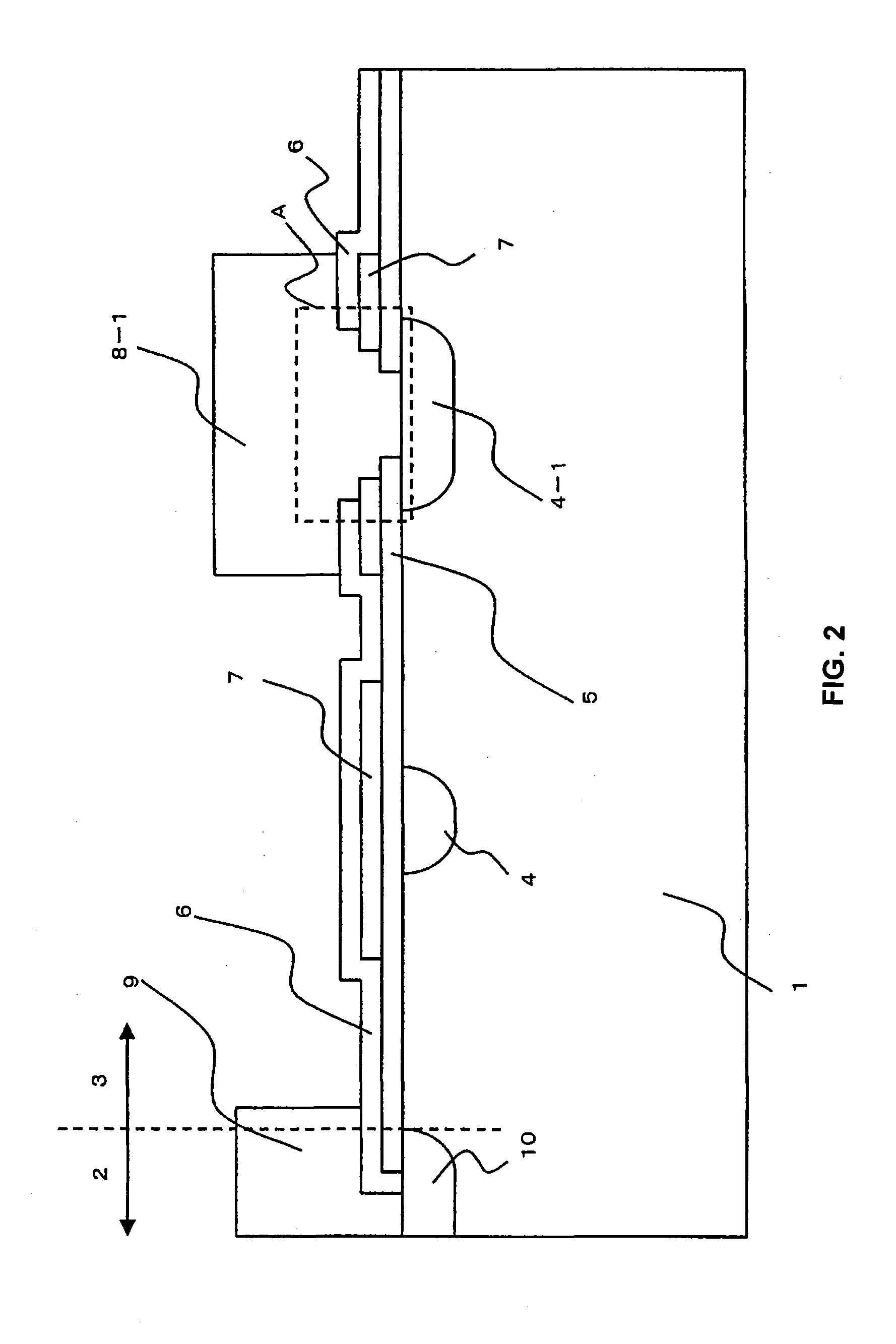
[0050]FIGS. 1 to 4 are essential part cross-sectional views of different edge termination structures of the power semiconductor device of the present invention. FIGS. 5 to 7 are cross-sectional views of different edge termination structures in the corner portion of the power semiconductor device of the present invention. FIG. 8 is an enlarged cross-sectional view of the edge termination structure in the corner portion of the power semiconductor device of the present invention. FIGS. 9 to 12 are cross-sectional views along the line X-X′ of the edge termination structure of FIG. 6B which serves to illustrate the method of fabricating the power semiconductor device of the present invention. FIG. 13 is a cross-sectional view along the line Y-Y′ of FIG. 6B which shows a non-contact portion of the edge termination structure in the corner portion of the power semiconductor device of the present invention. FIG. 15 is a (fifth) planar view B of the edge termination structure in the corner po...
PUM
 Abstract
Description
Claims
Application Information
 - Generate Ideas
- Intellectual Property
- Life Sciences
- Materials
- Tech Scout
- Unparalleled Data Quality
- Higher Quality Content
- 60% Fewer Hallucinations
Browse by: Latest US Patents, China's latest patents, Technical Efficacy Thesaurus, Application Domain, Technology Topic, Popular Technical Reports.
© 2025 PatSnap. All rights reserved.Legal|Privacy policy|Modern Slavery Act Transparency Statement|Sitemap|About US| Contact US: help@patsnap.com