

Image forming apparatus
a technology of image forming apparatus and control technique, which is applied in the direction of electrographic process apparatus, instruments, optics, etc., can solve the problems of poor image and poor transfer
- Summary
- Abstract
- Description
- Claims
- Application Information
AI Technical Summary
Benefits of technology
Problems solved by technology
Method used
Image

Examples
first embodiment
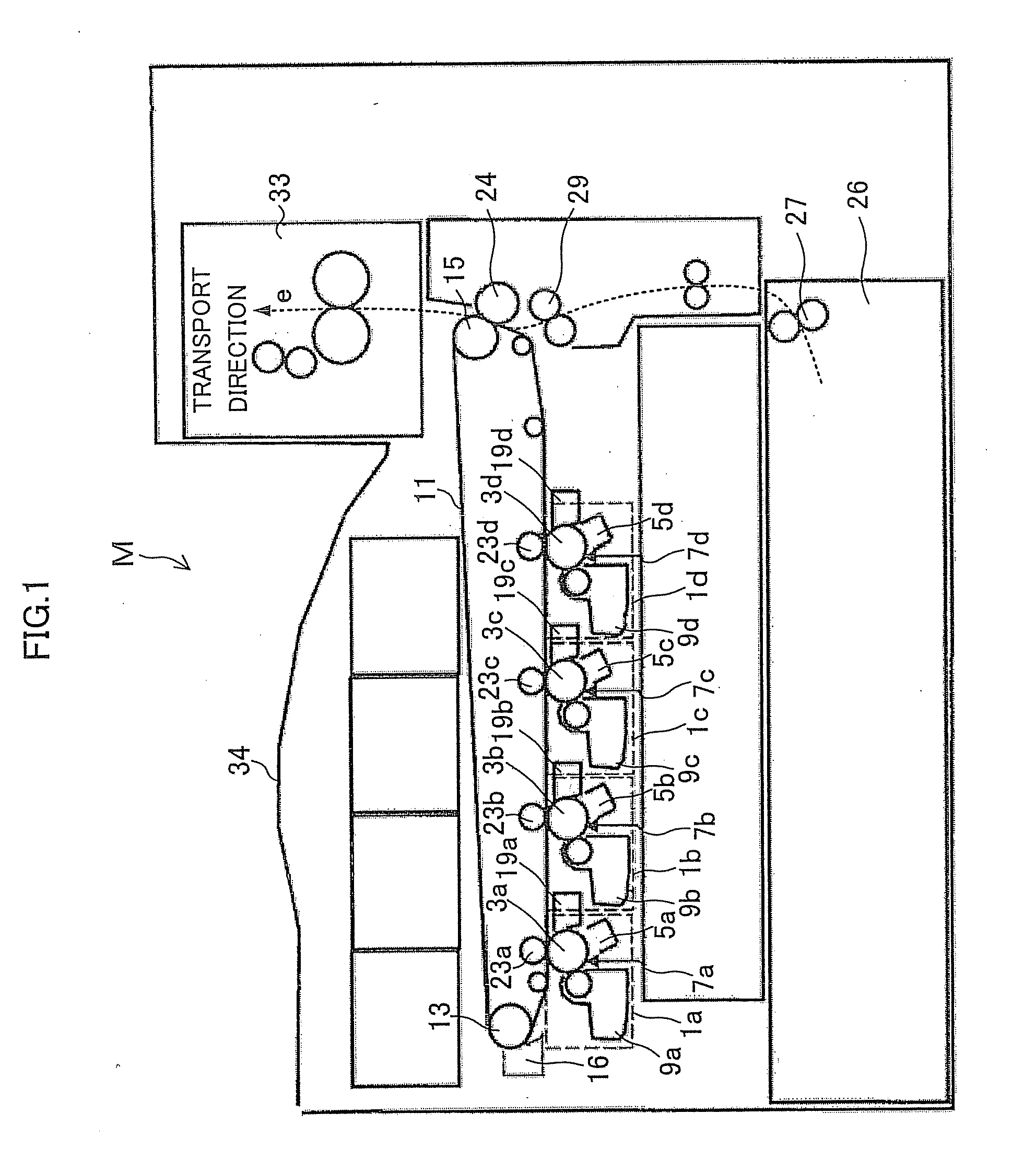
[0031]FIG. 1 is a longitudinal sectional view showing a schematic structure of an image forming apparatus M according to a first embodiment of the invention.
[0032]As shown in the drawing, the image forming apparatus M is provided with process units 1a, 1b, 1c and 1d as image forming means. The respective process units include photoconductive drums 3a, 3b, 3c and 3d as image bearing bodies, and developer images are formed on these photoconductors.
[0033]The process unit la will be described. In FIG. 1, the photoconductive drum 3a has a cylindrical shape with a diameter of 30 mm, and is provided to be rotatable in a clockwise direction in the drawing.
[0034]The following are provided around the photoconductive drum 3a along the rotation direction. First, a charging charger 5a is provided to be opposite to the surface of the photoconductive drum 1a. The charging charger 5a uniformly negatively (−) charges the photoconductive drum 3a. An exposure device 7a to expose the charged photocondu...
second embodiment
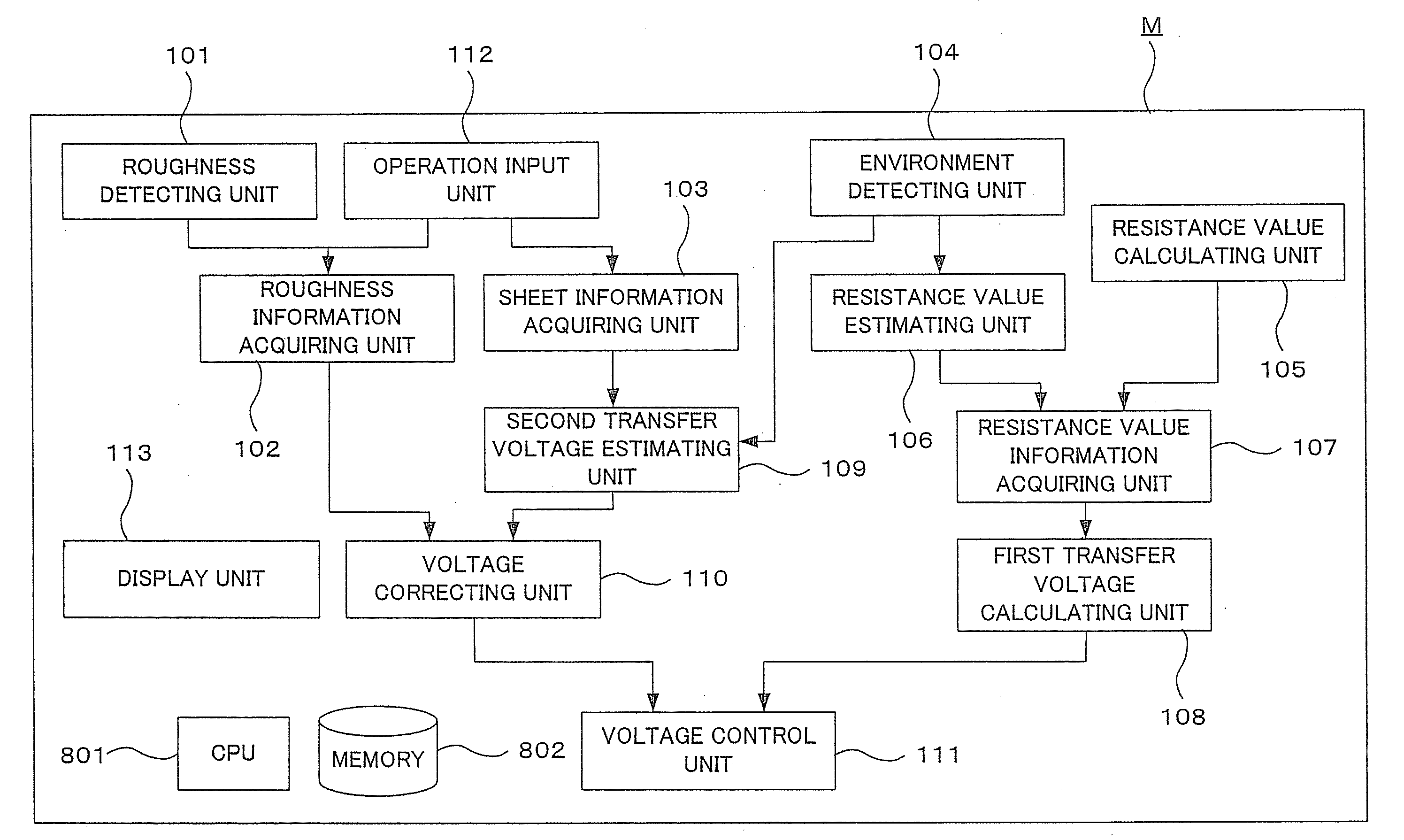
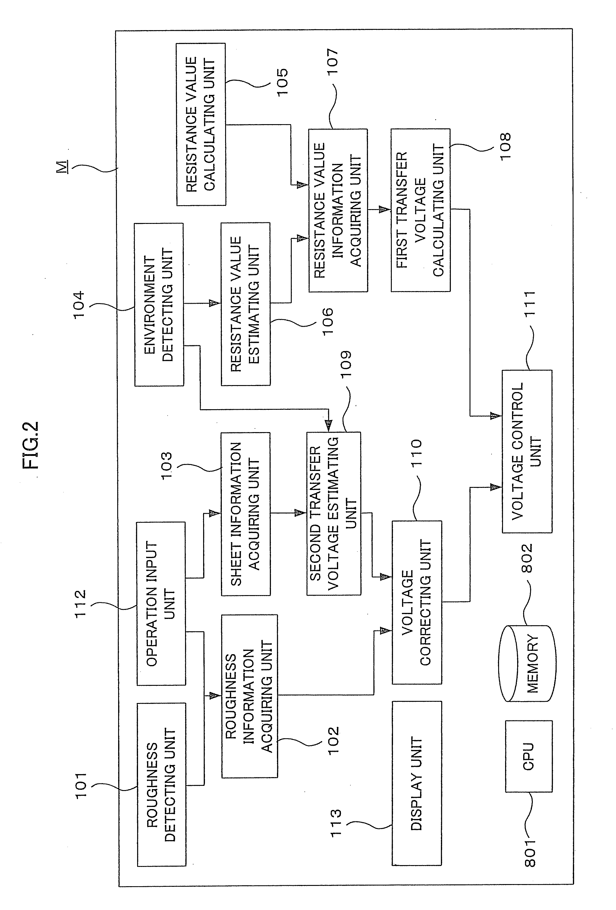
[0100]Next, a second embodiment of the invention will be described. This embodiment is a modified example of the first embodiment, and the structure of a secondary transfer unit in an image forming apparatus of this embodiment is similar to that of the first embodiment as shown in FIG. 15.
[0101]In this embodiment, a relative humidity sheet correction voltage table is not used, and as shown in FIG. 15 and FIG. 16, in a state where the sheet is nipped in the secondary transfer unit, the electric resistance detection of the secondary transfer unit is performed, the obtained voltage is made Vb, a correction voltage of the sheet is directly acquired from Vb−Va, and a specified voltage for toner is added to obtain a sheet correction voltage Vc. Here, similarly to the foregoing embodiment, in the case where the value of the surface roughness of the sheet is different from a specified value, the sheet correction voltage is corrected according to the difference.
[0102]For example, in the case...
third embodiment
[0113]Next, an image forming apparatus according to a third embodiment of the invention will be described.
[0114]In this embodiment, by using the surface roughness of the sheet, the transfer bias voltage can be determined more precisely than the foregoing embodiment.
[0115]First, the surface roughness of the sheet is detected by the roughness detecting unit. It is preferable that the detection of the surface roughness of the sheet is performed in the vicinity of a position where the sheet is nipped by register rollers. The detection of the surface roughness is performed such that the sheet surface is two-dimensionally grasped as a grayscale picture by a CMOS sensor, and is converted into roughness information by an image processing. The optimum transfer current is determined by referring to a previously defined relation between a sheet surface roughness and a suitable transfer current. For example, in an “A” sheet with a surface roughness of about 1.4 μm, the suitable transfer current...
PUM
 Abstract
Description
Claims
Application Information