Circuit and Method for Physical Defect Detection of an Integrated Circuit

Inactive Publication Date: 2008-07-31
QIMONDA
View PDF3 Cites 12 Cited by
  • Summary
  • Abstract
  • Description
  • Claims
  • Application Information

AI Technical Summary

Benefits of technology

[0005]The test circuit may take on any of a number of forms. In one embodiment, the test circuit comprises at least one pull-down transistor that is connected to the dedicated conductive test

Problems solved by technology

If there is no continuity on the conductive test path, then the device is said to have physical damage since a break in th

Method used


Image

  • Circuit and Method for Physical Defect Detection of an Integrated Circuit
  • Circuit and Method for Physical Defect Detection of an Integrated Circuit
  • Circuit and Method for Physical Defect Detection of an Integrated Circuit

Examples


Embodiment Construction

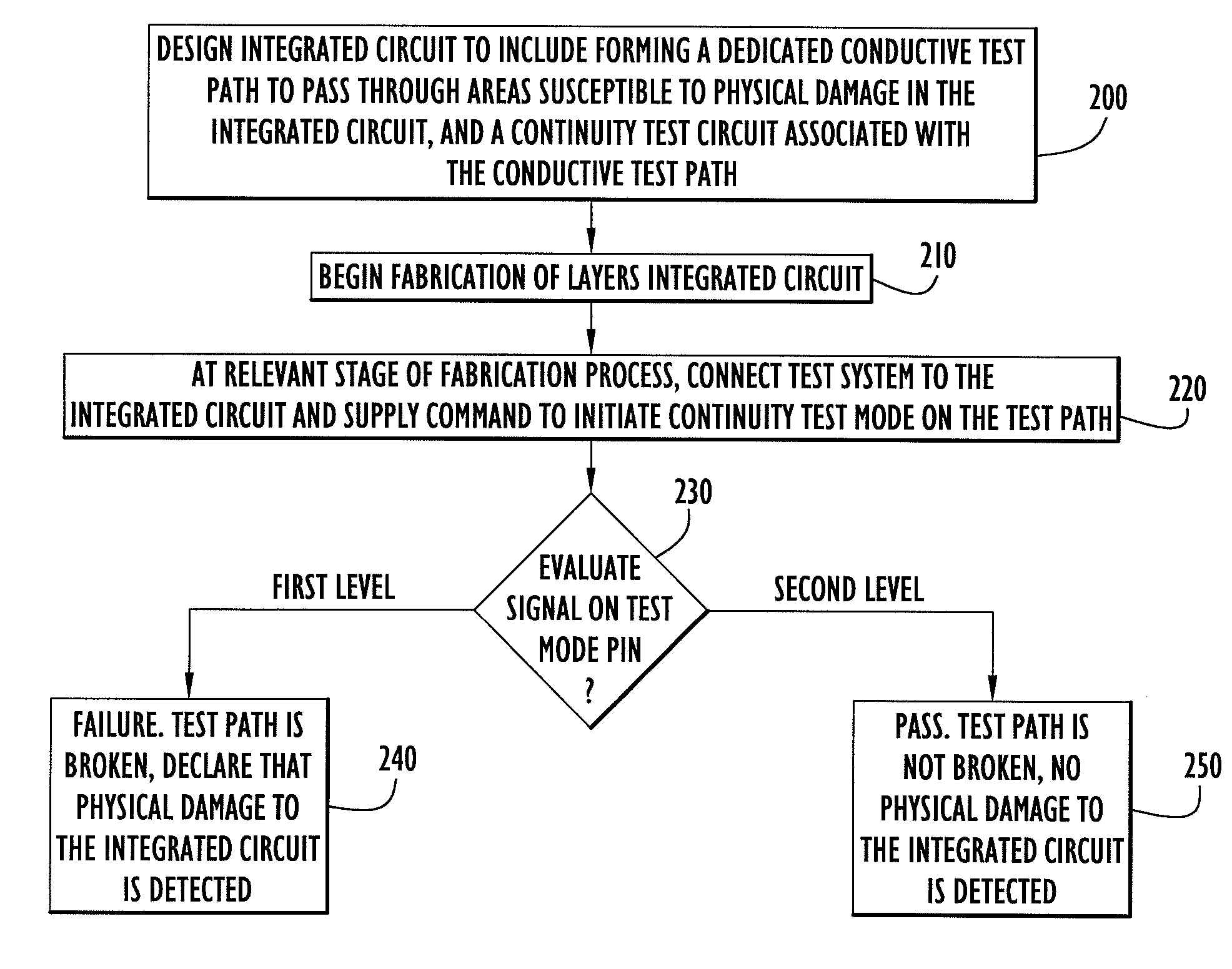
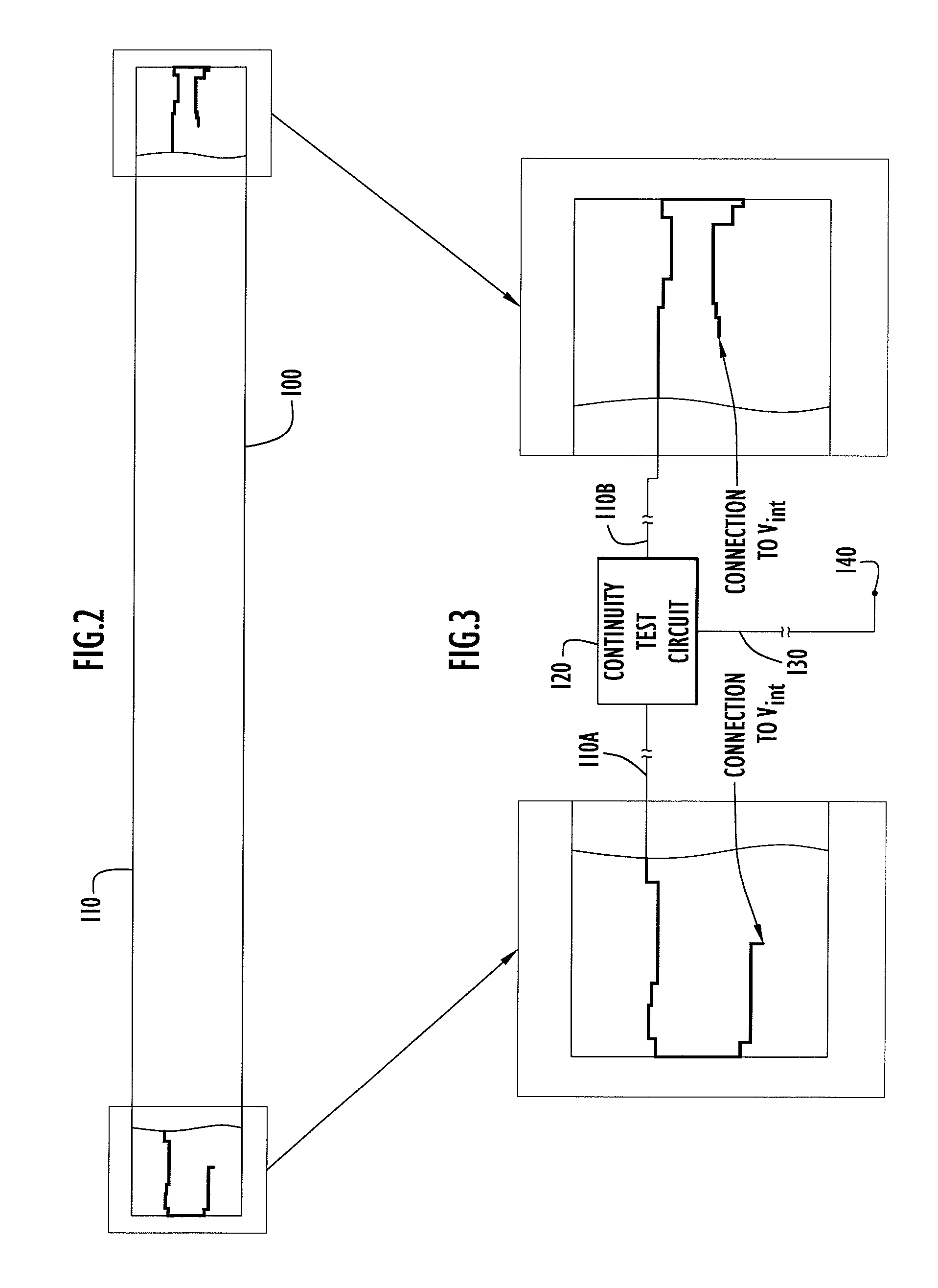
[0012]According to the present invention, a capability is provided to test or screen semiconductor integrated circuit devices for physical damage during and after fabrication without disassembling and destroying the integrated circuit device. Thus, a device can be tested for physical damage without destroying the device so that if the device passes the physical damage test, it can be sent to a customer with a higher confidence that it will not be returned due to degradation as a result of a physical damage failure.

[0013]In one embodiment, a conductive line is included in the design of an integrated circuit. The conductive line is a dedicated conductive test path that is used for testing for physical damage caused during fabrication. A test circuit is also provided (or may already exist) in the design of the integrated circuit. The test circuit is connected to the dedicated conductive test path to test for continuity of the conductive test path. When there is a break in the conductiv...


PUM


Abstract

A semiconductor integrated circuit device having a physical damage testing capability and a method for testing for physical damage caused during fabrication, assembly or test of the semiconductor integrated circuit are provided. A dedicated conductive test path is formed during fabrication of the integrated circuit device. The test path is routed to pass through areas of the integrated circuit which are susceptible to physical damage. A test circuit is included in the integrated circuit and is connected to the dedicated conductive test path. The test circuit tests the dedicated conductive test path for a characteristic indicative of physical damage. In one embodiment, the test circuit is a continuity circuit that measures whether there is continuity on the conductive test path. The continuity test circuit is activated in response to an externally supplied test command, such as from a test system, and to supply an output signal to a pad that is externally readable by the test system.

Description

BACKGROUND OF THE INVENTION[0001]Fabrication of semiconductor integrated circuit devices involves numerous complex steps in extremely thin material. During certain steps of the fabrication process, areas of the integrated circuit are placed under physical stress that may cause physical damage to the device. For example, and not by way of limitation, devices that use a ball grid array (BGA) endure heat and mechanical stress from a solder stop mask during part of the assembly process that can cause physical damage in the form of “metal peeling” near a bond channel at the edges of the semiconductor integrated circuit die.[0002]Currently, there is no way to test a device for physical damage during or after the fabrication process without taking the device apart which renders it completely dysfunctional. As a result, devices with physical damage may leave the factory if the physical damage does not otherwise present itself in other defects that can be detected in functional tests.[0003]W...

Claims


Application Information

Patent Timeline
IPC IPC(8): G01R31/3181G06F11/26
CPCG01R31/31722G01R31/318357G01R31/318342G01R31/31723
Inventor ISOM, MELVINMANN, STEPHEN
Owner QIMONDA
Why Eureka
Try Eureka