Solid-state image-pickup device signal processing apparatus

a solid-state image and signal processing technology, applied in the direction of color television details, television system details, television systems, etc., can solve the problems of difficult miniaturization and deterioration of signal level accuracy, and achieve the effect of simplified circuits, less noise, and higher signal level accuracy

Inactive Publication Date: 2007-11-22
JAI
View PDF11 Cites 1 Cited by
  • Summary
  • Abstract
  • Description
  • Claims
  • Application Information

AI Technical Summary

Benefits of technology

[0021]According to the present invention, the following effects are exhibited.
[0022]1. According to the invention of claim 1 of the present invention,
[0023]And since a plurality of sample-hold circuits and amplifiers can be omitted, circuits are simplified and therefore there is not a problem specific to an analog circuit such as droop or the like of a sample-hold circuit and further it is possible to make a signal level higher in accuracy by making noises lower and make the apparatus more small-sized.
[0024]2. According to the invention of claim 2 of the present invention,
[0025]3. According to the invention of claim 3 of the present invention,
[0026]And even in case that picture element defects such as white flaws, black flaws and the like of a solid-state image-pickup device newly occur due to cosmic rays in the course of transportation using an aircraft or the like in particular, an on-site compensation is possible, and operations such as replacement, readjustment and the like of a solid-state image-pickup device can be omitted and thereby it is possible to greatly reduce the cost and shorten the period for delivery.

Problems solved by technology

As shown in the conventional example, since an analog correlated double sampling circuit uses many analog circuits assembled with discrete components such as a field-through S / H circuit for sample-holding a field-through level tF period for each picture element, similarly a video signal S / H circuit for sample-holding a video signal tS period for each picture element, a differential amplifier and the like, miniaturization of it has been difficult.
And deterioration in accuracy of a signal level caused by occurrence of droop and the like due to inter-electrode capacitance and the like of semiconductor parts in an S / H circuit and circuit noises due to the complexity of a circuit configuration have not been able to be neglected.

Method used


Image

  • Solid-state image-pickup device signal processing apparatus
  • Solid-state image-pickup device signal processing apparatus
  • Solid-state image-pickup device signal processing apparatus

Examples


Embodiment Construction

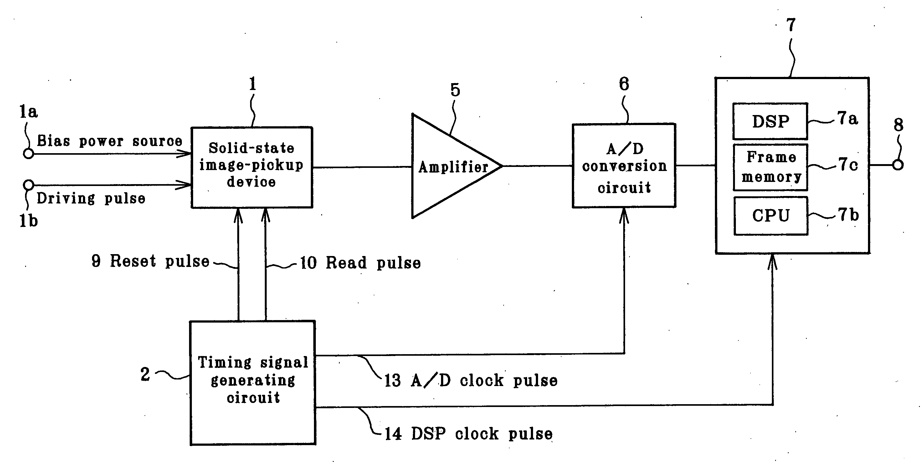
[0042]An embodiment of a solid-state image-pickup device signal processing apparatus of the present invention is described on the basis of drawings of the embodiment. Parts corresponding to FIGS. 5 and 6 are given the same symbols.

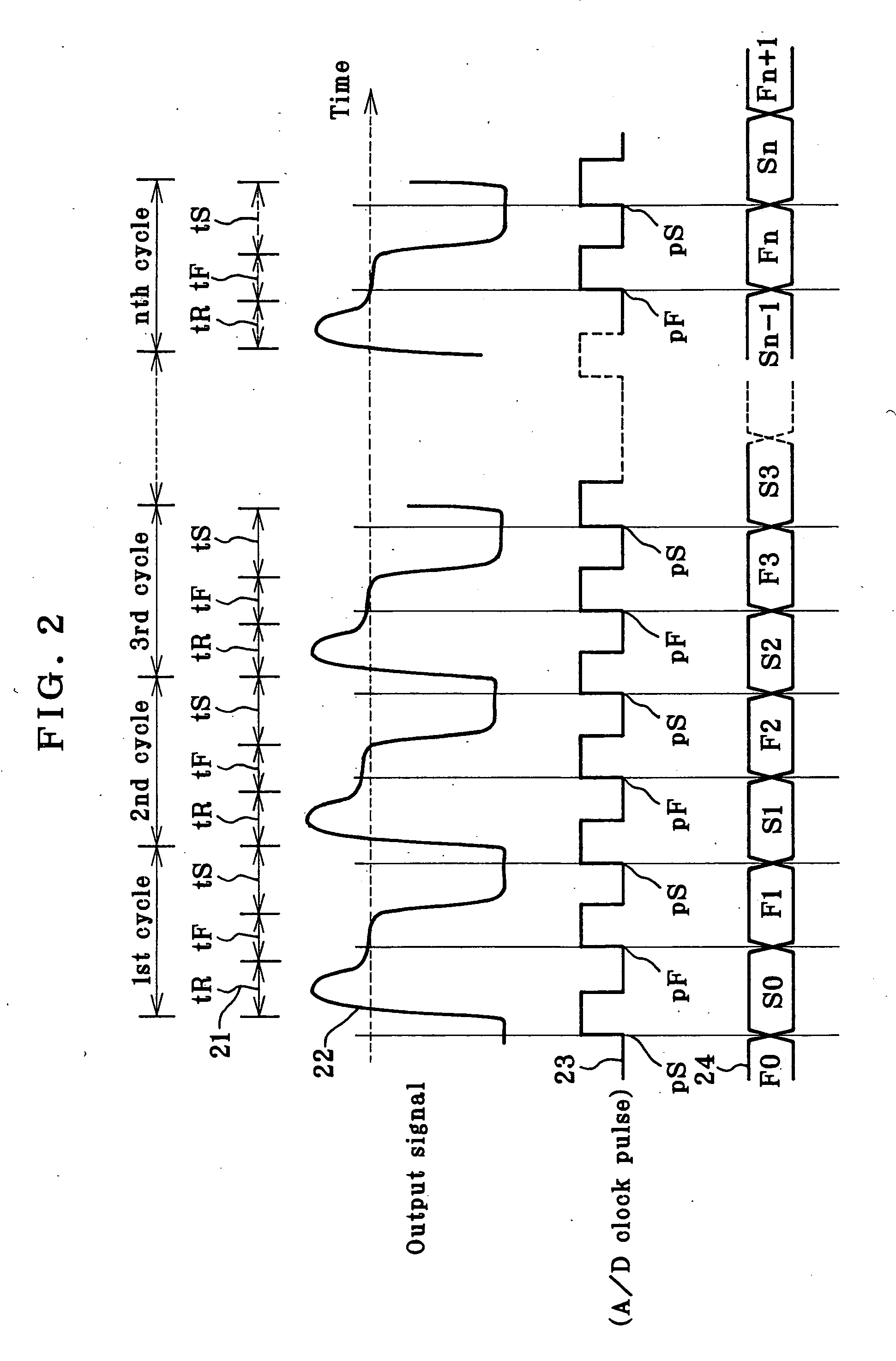
[0043]FIG. 1 is a block diagram of a solid-state image-pickup device signal processing apparatus of an embodiment of the present invention, FIG. 2 is an output waveform and digitized signal waveform diagram of a solid-state image-pickup device of the same embodiment of the present invention, FIG. 3 is a schematic diagram for explaining a digital correlated double sampling operation and an operation of adding an optional-value direct current signal to said video signal portion, and FIG. 4 is a schematized waveform diagram using digital values of the digital correlated double sampling of the same embodiment of the present invention.

[0044]In FIG. 1, a solid-state image-pickup device signal processing apparatus of an embodiment of the present invention is comp...


PUM


Abstract

To provide a digital correlated double sampling circuit having a plurality of functions such as flaw compensation, shading compensation and the like specific to CCD, said functions being added to a correlated double sampling circuit.
A solid-state image-pickup device signal processing apparatus comprising a solid-state image-pickup device, an amplifier for amplifying an output signal of said solid-state image-pickup device, an D/A conversion circuit for converting an-analog output signal of said amplifier to a digital signal and a digital correlated double sampling circuit for removing noises by performing a subtraction process between a field-through portion and its directly subsequent video signal portion of a digital output signal of said D/A conversion circuit, wherein said digital correlated double sampling circuit has an optional-value direct current signal added to said video signal portion and variably controls said optional-value direct current signal for each frame or each of said video signal portions.

Description

BACKGROUND ART[0001]The present invention relates to signal processing of a solid-state image-pickup device, and more particularly to a solid-state image-pickup device signal processing apparatus using a digital correlated double sampling circuit.[0002]A conventional example related to a CCD of a television camera using a solid-state image-pickup device (hereinafter, described as CCD) in general and a correlated double sampling circuit is shown in FIG. 5 and FIG. 6.[0003]In a block diagram of a solid-state image-pickup device signal processing apparatus of a conventional example shown in FIG. 5, a CCD 1 has a bias power source supplied at a bias power source input terminal 1a and a driving pulse supplied at a driving pulse input terminal 1b. And the CCD 1 is operated as publicly known by being supplied with a reset pulse and a read pulse generated by a timing signal generating circuit (hereinafter, described as TSG) 2.[0004]In an output waveform diagram of a conventional solid-state...

Claims


Application Information

Patent Timeline
Patent Type & Authority Applications(United States)
IPC IPC(8): H04N5/247
CPCH04N5/3572H04N5/3575H04N5/361H04N5/372H04N5/3651H04N5/367H04N5/363H04N25/616H04N25/61H04N25/63H04N25/65H04N25/671H04N25/68H04N25/71
Inventor TAKAHASHI, ISAO
Owner JAI
Why Eureka
Try Eureka