Fin Pin Diode

a junction diode and pin diode technology, applied in the field of semiconductor devices, can solve the problems of reducing the sensitivity of the pin diode to light, reducing the cost of forming the pin diode, and complicating the challenge of efficiently forming the vertical pin diod

Inactive Publication Date: 2008-08-07
IBM CORP
View PDF8 Cites 71 Cited by
  • Summary
  • Abstract
  • Description
  • Claims
  • Application Information

AI Technical Summary

Problems solved by technology

In the case of laterally formed PIN diodes, reducing feature size results in a limited junction area between the p, i, and n layers, thereby reducing the sensitivity of the PIN diode to light, for example.
While forming PIN diodes in deep trenches enhances junction area, and therefore diode sensitivity, the process for forming the PIN diodes is relatively complicated and costly.
Furthermore, the emergence of Fin Field Effect Transistor (FinFET) technology has further complicated the challenge to efficiently form vertical PIN diodes.
However, using FinFET based technology requires the redesign of vertical PIN diodes.

Method used


Image

  • Fin Pin Diode
  • Fin Pin Diode
  • Fin Pin Diode

Examples


Embodiment Construction

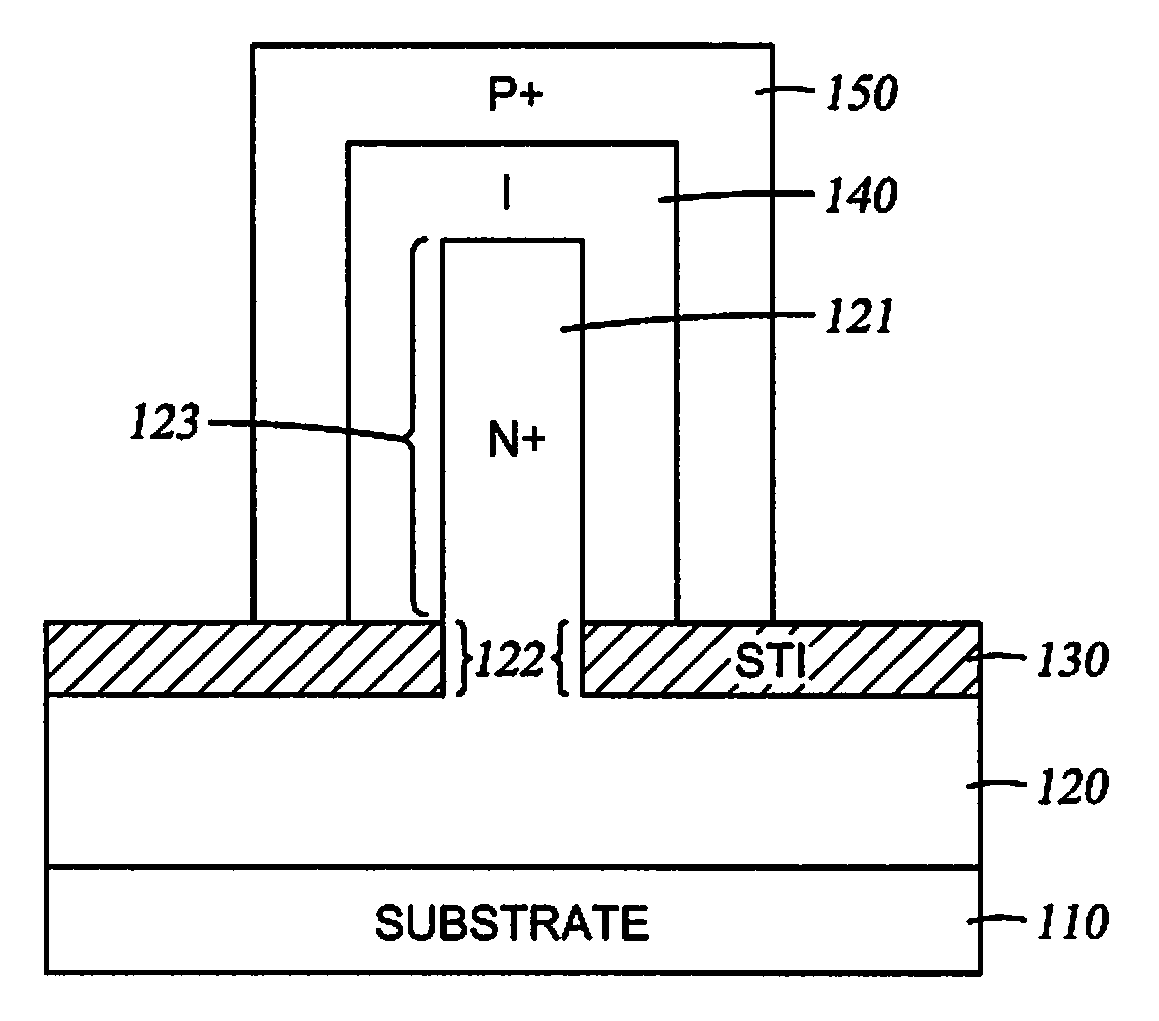
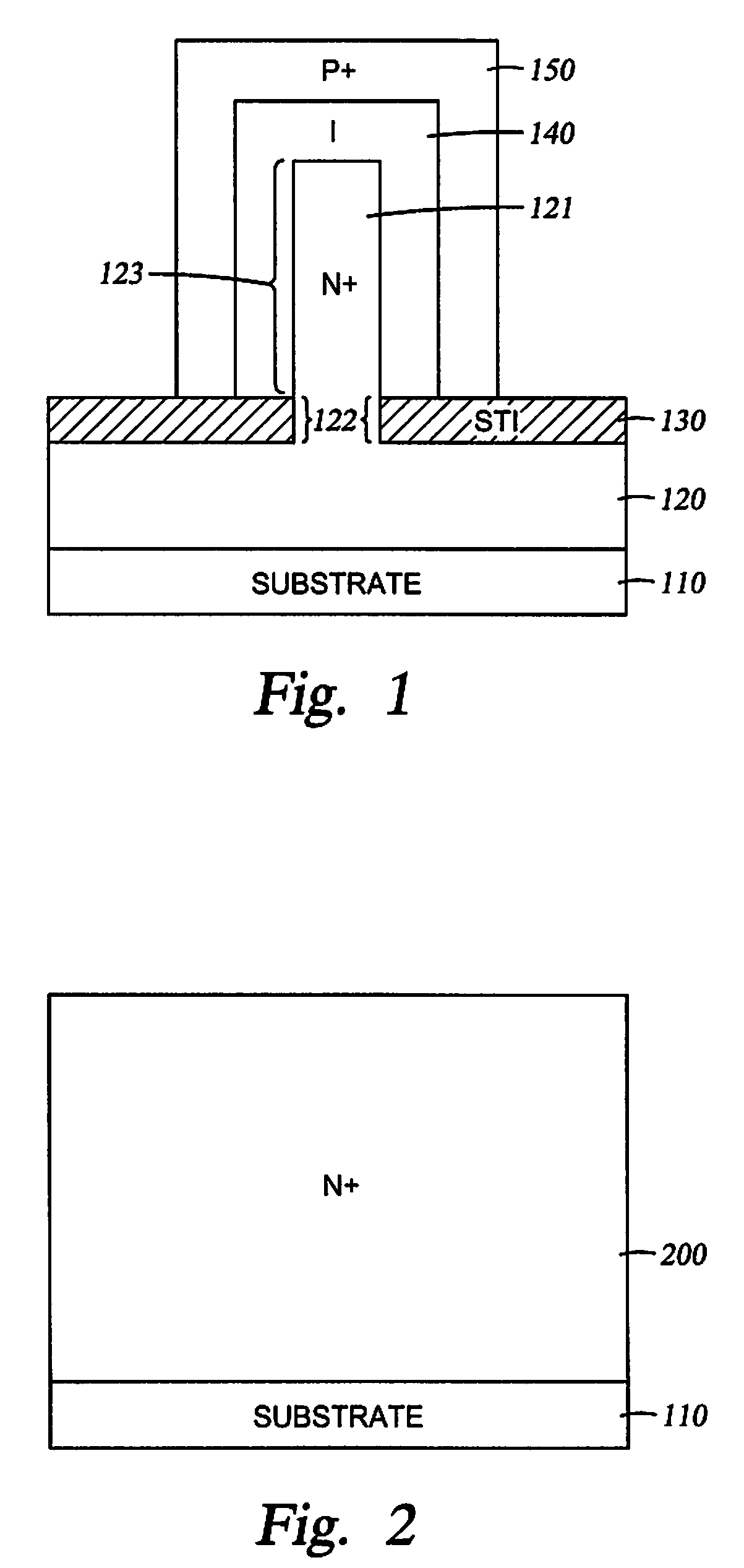
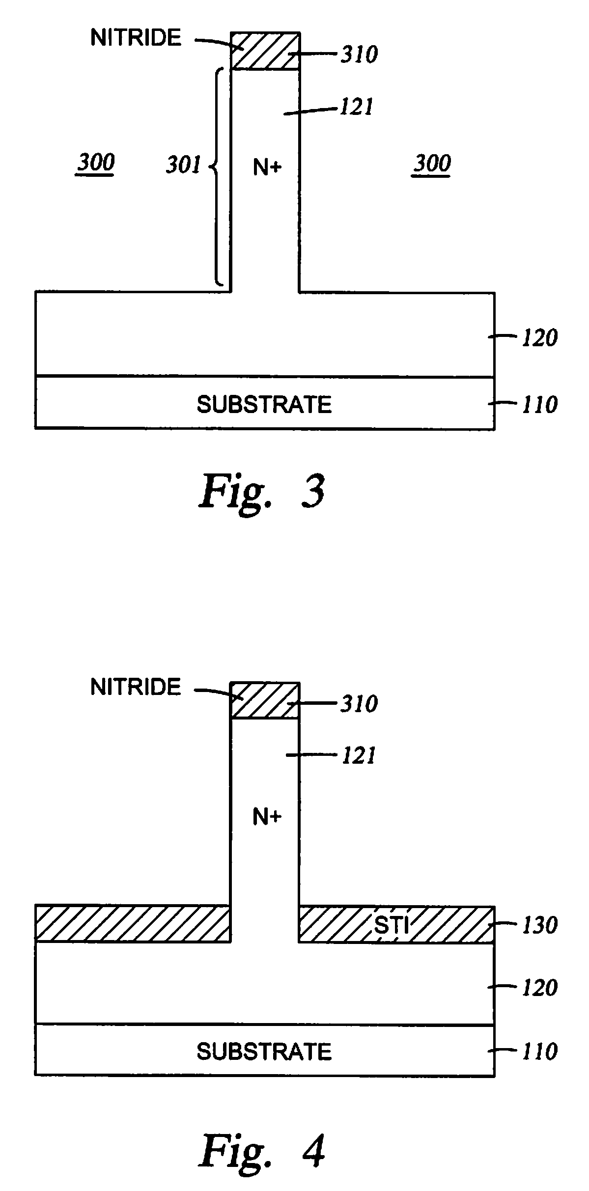
[0035]The present invention generally relates to the field of semiconductor devices, and more specifically to fin-based junction diodes. A doped semiconductor fin may protrude from a first doped layer. An intrinsic layer may be formed adjacent to and surrounding the semiconductor fin. A second semiconductor layer may be formed adjacent to and surrounding the intrinsic layer, thereby forming a PIN diode compatible with FinFET technology and having increased junction area.

[0036]In the following, reference is made to embodiments of the invention. However, it should be understood that the invention is not limited to specific described embodiments. Instead, any combination of the following features and elements, whether related to different embodiments or not, is contemplated to implement and practice the invention. Furthermore, in various embodiments the invention provides numerous advantages over the prior art. However, although embodiments of the invention may achieve advantages over ...


PUM


Abstract

Embodiments of the invention generally relate to the field of semiconductor devices, and more specifically to fin-based junction diodes. A portion of a doped semiconductor fin may protrude through a first doped layer. An intrinsic layer may be disposed on the protruding semiconductor fin. A second semiconductor layer may be disposed on the intrinsic layer, thereby forming a PIN diode compatible with FinFET technology and having increased junction area.

Description

BACKGROUND OF THE INVENTION[0001]1. Field of the Invention[0002]The present invention generally relates to the field of semiconductor devices, and more specifically to Fin-based junction diodes.[0003]2. Description of the Related Art[0004]Junction diodes, for example, PIN diodes are commonly used in a wide variety of products such as Radio Frequency (RF) switching devices, telecommunication products, Electrostatic Discharge (ESD) protect devices, imaging sensors, and the like.[0005]The application of PIN diodes may also be extended to photodetectors or optical receivers for emerging optical interconnect technology. For example, when light is illuminated on a PIN photodiode, a current may be generated in the PIN photodiode based on the intensity of the light. When no light is present, the PIN photodiode may be reverse biased, and almost no current may be generated in the PIN photodiode. Therefore, PIN photodiodes are capable of detecting optical signals.[0006]PIN diodes are typically...

Claims


Application Information

Patent Timeline
Patent Type & Authority Applications(United States)
IPC IPC(8): H01L29/868H01L21/329
CPCH01L29/0649H01L29/868H01L29/66136H01L29/417
Inventor CHENG, KANGGUOHSU, LOUIS LU-CHENMANDELMAN, JACK ALLAN
Owner IBM CORP
Why Eureka
Try Eureka