Light Emitting Device and Method of Manufacturing the Same

a technology of light emitting device and manufacturing method, which is applied in the details of semiconductor/solid-state devices, electric lighting sources, solid-state devices, etc., can solve the problems of increased manufacturing costs, flicker effect according to the arrangement, and cumbersome installation of additional auxiliary circuits

Inactive Publication Date: 2008-08-14
SEOUL VIOSYS CO LTD
View PDF8 Cites 44 Cited by
  • Summary
  • Abstract
  • Description
  • Claims
  • Application Information

AI Technical Summary

Problems solved by technology

However, when the aforementioned light emitting device with a flip-chip structure is driven under a household AC power source, a flicker effect occurs according to on / off at 50 to 60 Hz in the AC power source.
Thus, there is cumbersomeness in that an additional auxiliary circuit should be mounted.
Accordingly, there is a disadvantage in that manufacturing costs rise due to increases in processing time and costs.

Method used


Image

  • Light Emitting Device and Method of Manufacturing the Same
  • Light Emitting Device and Method of Manufacturing the Same
  • Light Emitting Device and Method of Manufacturing the Same

Examples


Embodiment Construction

[0030]Hereinafter, preferred embodiments of the present invention will be described in detail with reference to the accompanying drawings. However, the present invention is not limited to the embodiments but may be implemented into different forms. These embodiments are provided only for illustrative purposes and for full understanding of the scope of the present invention by those skilled in the art. Throughout the drawings, like elements are designated by like reference numerals.

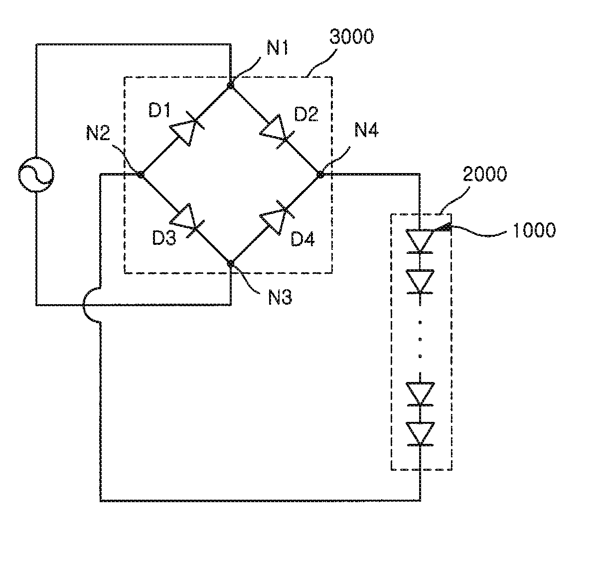
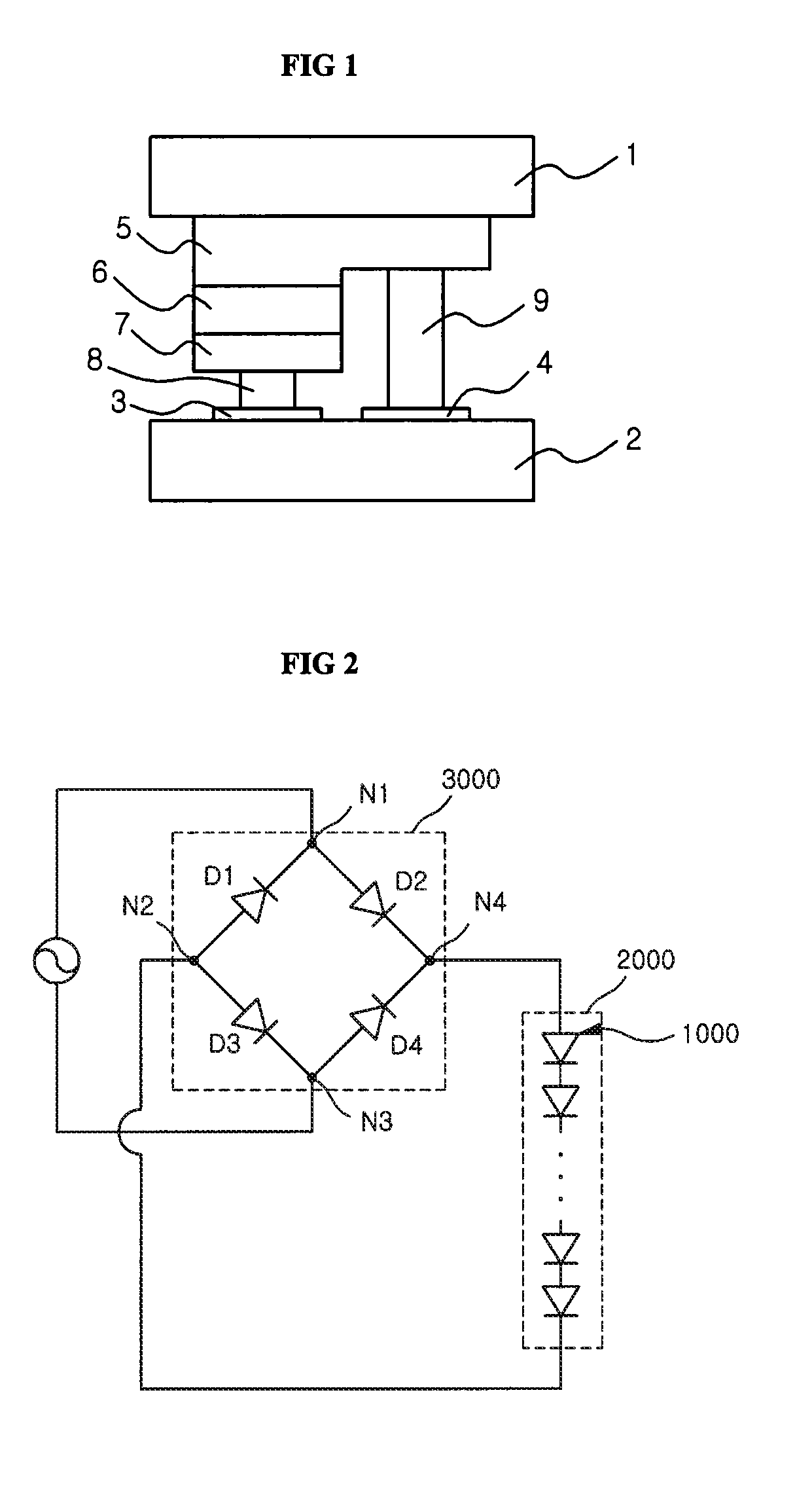
[0031]FIG. 2 is a conceptual circuit diagram illustrating a light emitting device according to the present invention.

[0032]Referring to this figure, the light emitting device comprises a light emitting cell block 2000 having a plurality of light emitting cells 1000 connected in series, and a rectifying bridge 3000 for applying a predetermined current to the light emitting cell block 2000. In this embodiment, the light emitting cell block 2000 having the plurality of light emitting cells 1000 connected in s...


PUM


Abstract

The present invention provides a light emitting device comprising a first semiconductor substrate including a light emitting cell block having a plurality of light emitting cells connected in series on one surface thereof; a second semiconductor substrate having one surface formed with a rectifying bridge and the other surface bonded to the other surface of the first semiconductor substrate; and a submount substrate to which the second semiconductor substrate is flip-chip bonded to be in contact with the one surface of the second semiconductor substrate, wherein rectified power is applied to the light emitting cell block through the rectifying bridge. The present invention further provides a method of manufacturing the light emitting device. The light emitting device and the method of manufacturing the same according to the present invention have advantages in that a flicker effect generated from an AC power source can be minimized and constant brightness can be maintained even in changes in the voltage of the AC power source by integrating a rectifying circuit into a light emitting device with a flip-chip structure, and in that there is no cumbersomeness of mounting an additional auxiliary device, resulting in increase of the degree of utilization of space and improved light output.

Description

RELATED APPLICATIONS[0001]This application is a U.S. national phase application of PCT International Application No. PCT / KR2006 / 003095, filed Aug. 7, 2006, which claims priority of Korean Patent Application No. 2005-073284, filed Aug. 10, 2005, the contents of which are incorporated herein by reference in their entirety.FIELD OF THE INVENTION[0002]The present invention relates to a light emitting device and a method of manufacturing the same, and more particularly, to a light emitting device with a flip-chip structure, which can improve the degree of integration of elements and reduce a flicker effect due to an alternating current (AC) in the light emitting device, and a method of manufacturing the light emitting device.BACKGROUND OF THE INVENTION[0003]A light emitting diode (LED) refers to an element in which minority carriers (electrons or holes) injected using a p-n junction structure of a semiconductor are produced and certain light is emitted through recombination thereof. Ligh...

Claims


Application Information

Patent Timeline
Patent Type & Authority Applications(United States)
IPC IPC(8): H05B37/00H01L33/00H01L33/08H01L33/22H01L33/32H01L33/62
CPCH01L25/0756H01L27/153H01L33/22H01L2924/0002H01L2924/00
Inventor LEE, JAE HO
Owner SEOUL VIOSYS CO LTD
Why Eureka
Try Eureka