Chip holder with wafer level redistribution layer

a technology of redistribution layer and chip holder, which is applied in the direction of semiconductor/solid-state device details, semiconductor devices, electrical apparatus, etc., can solve the problems of reducing the ability to continue to shrink the size of the semiconductor chip, and the bond pads for connecting the semiconductor chip to external features become smaller and more tightly packed

Inactive Publication Date: 2008-08-21
TAIWAN SEMICON MFG CO LTD
View PDF32 Cites 11 Cited by
  • Summary
  • Abstract
  • Description
  • Claims
  • Application Information

AI Technical Summary

Problems solved by technology

While the increase in integration levels and advances in miniaturization provide semiconductor chips that can store more data, perform more functions and are smaller in size, an undesirable by-product of such a decrease in semiconductor chip size is that the bond pads for connecting the semiconductor chip to external feature...

Method used


Image

  • Chip holder with wafer level redistribution layer
  • Chip holder with wafer level redistribution layer
  • Chip holder with wafer level redistribution layer

Examples


Embodiment Construction

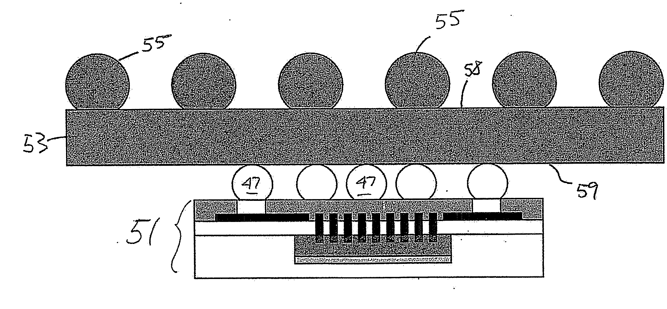
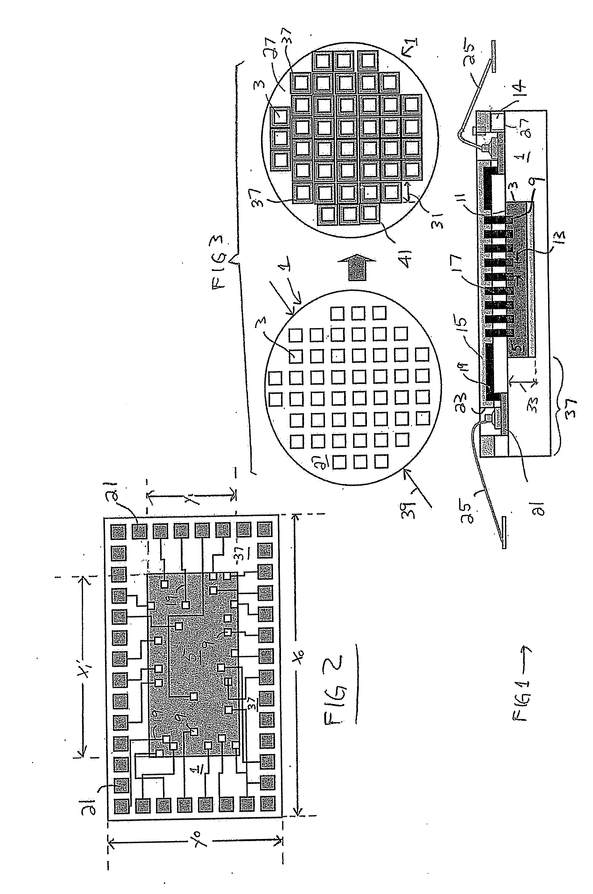
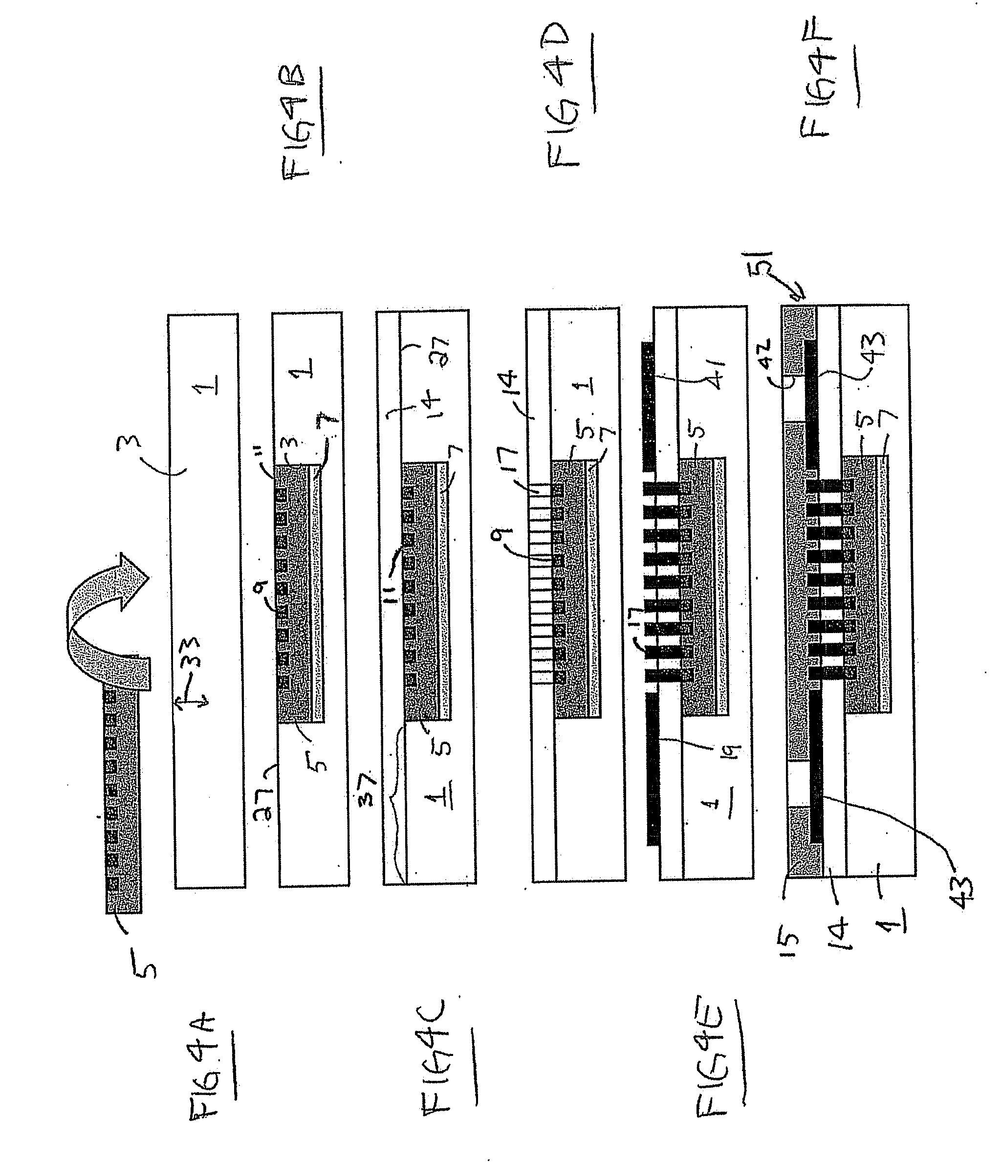
[0014]The present invention provides a method and structure for expanding the size and pitch of bond pads and increasing the bonding area upon which the bond pads are formed on a semiconductor chip, by providing a chip holder that retains the semiconductor chip and provides an expanded area that includes the bond pads coupled to the semiconductor chip by providing bond pads on or over the surface of the chip holder that retains the semiconductor chip. The semiconductor chip may then be packaged in the chip holder, which may alternatively be referred to as a carrier substrate.

[0015]The invention provides for inserting at least one semiconductor chip into a corresponding recess formed within the chip holder using automated die pick and placement equipment then processing the chip holder including one or more semiconductor chips using commercially available manufacturing and fabrication equipment used to fabricate the semiconductor chips themselves. The chip holders are sized and forme...


PUM


Abstract

A chip holder formed of silicon, glass, other ceramics or other suitable materials includes a plurality of recesses for retaining semiconductor chips. The bond pads of the semiconductor chip are formed on or over an area of the chip holder that surrounds the semiconductor chip thus expanding the bonding area. The bond pads are coupled, using semiconductor wafer processing techniques, to internal bond pads formed directly on the semiconductor chip.

Description

FIELD OF THE INVENTION[0001]The present invention generally relates to semiconductor manufacturing and packaging, and more particularly to using a carrier substrate, i.e. chip holder to increase the pitch of bond pads for a semiconductor chip.BACKGROUND[0002]Increased miniaturization is an important goal in today's rapidly advancing semiconductor manufacturing industry. There is a push to reduce device feature sizes and to increase integration levels within a device as well as to reduce the size of the semiconductor chips themselves. CUP (circuit under pad) technologies have enabled the placement of bond pads anywhere on the semiconductor chip and also enabled additional bond pads to be packed in close proximity. While the increase in integration levels and advances in miniaturization provide semiconductor chips that can store more data, perform more functions and are smaller in size, an undesirable by-product of such a decrease in semiconductor chip size is that the bond pads for c...

Claims


Application Information

Patent Timeline
IPC IPC(8): H01L23/498H01L21/60
CPCH01L23/49816H01L2924/01047H01L24/19H01L2224/04105H01L2224/20H01L2224/92244H01L2924/01013H01L2924/01029H01L2924/01057H01L2924/01078H01L2924/09701H01L2924/15311H01L2924/19107H01L2924/01033H01L23/5389H01L2224/12105
Inventor CHEN, CHEN-SHIENYANG, CHAO-HSIANGLIANG, JIMMYTSENG, HAN-LIANGLII, MIRNG-JIKARTA, TJANDRA WINATAWU, HUA-SHU
Owner TAIWAN SEMICON MFG CO LTD
Why Eureka
Try Eureka