Defect detecting device, defect detecting method, image sensor device, image sensor module, defect detecting program, and computer-readable recording medium

a defect detection and defect technology, applied in image enhancement, image analysis, instruments, etc., can solve problems such as incongruity of inspection, difficult to detect defects, and complex changes in pixels values, so as to reduce erroneous determinations and accurate detection.

Inactive Publication Date: 2008-08-28
SHARP KK
View PDF12 Cites 33 Cited by
  • Summary
  • Abstract
  • Description
  • Claims
  • Application Information

AI Technical Summary

Benefits of technology

[0024]The foregoing makes it possible to detect the defects due to color change in the inspection-target image. Further, if the defects due to color change are present in either the vertical direction or the horizontal direction of the inspection-target image, the vertical line defects or the horizontal line defects are accurately detectable. Further,

Problems solved by technology

Especially in image-sensor images, presence of spot defects, unevenness defects, line defects and the like cause the pixels values to change in a complicated manner according to the respective defects with respect to the pixel coordinates.
It is therefore not easy to detect the defects.
This way of inspection depends on subjective judgment of the inspecting staff and therefore has a problem that the results of this inspection are not consistent because standards of the inspection vary among the inspecting staff or because of physical condition of the inspecting staff at the time of the inspection.
There is another problem that it is difficult with this way of inspection to quantify the defects.
However, with the smoothing process only, the impact of the noise components is still high.
Thus, in

Method used


Image

  • Defect detecting device, defect detecting method, image sensor device, image sensor module, defect detecting program, and computer-readable recording medium
  • Defect detecting device, defect detecting method, image sensor device, image sensor module, defect detecting program, and computer-readable recording medium
  • Defect detecting device, defect detecting method, image sensor device, image sensor module, defect detecting program, and computer-readable recording medium

Examples


Embodiment Construction

1. Basic Device Configurations

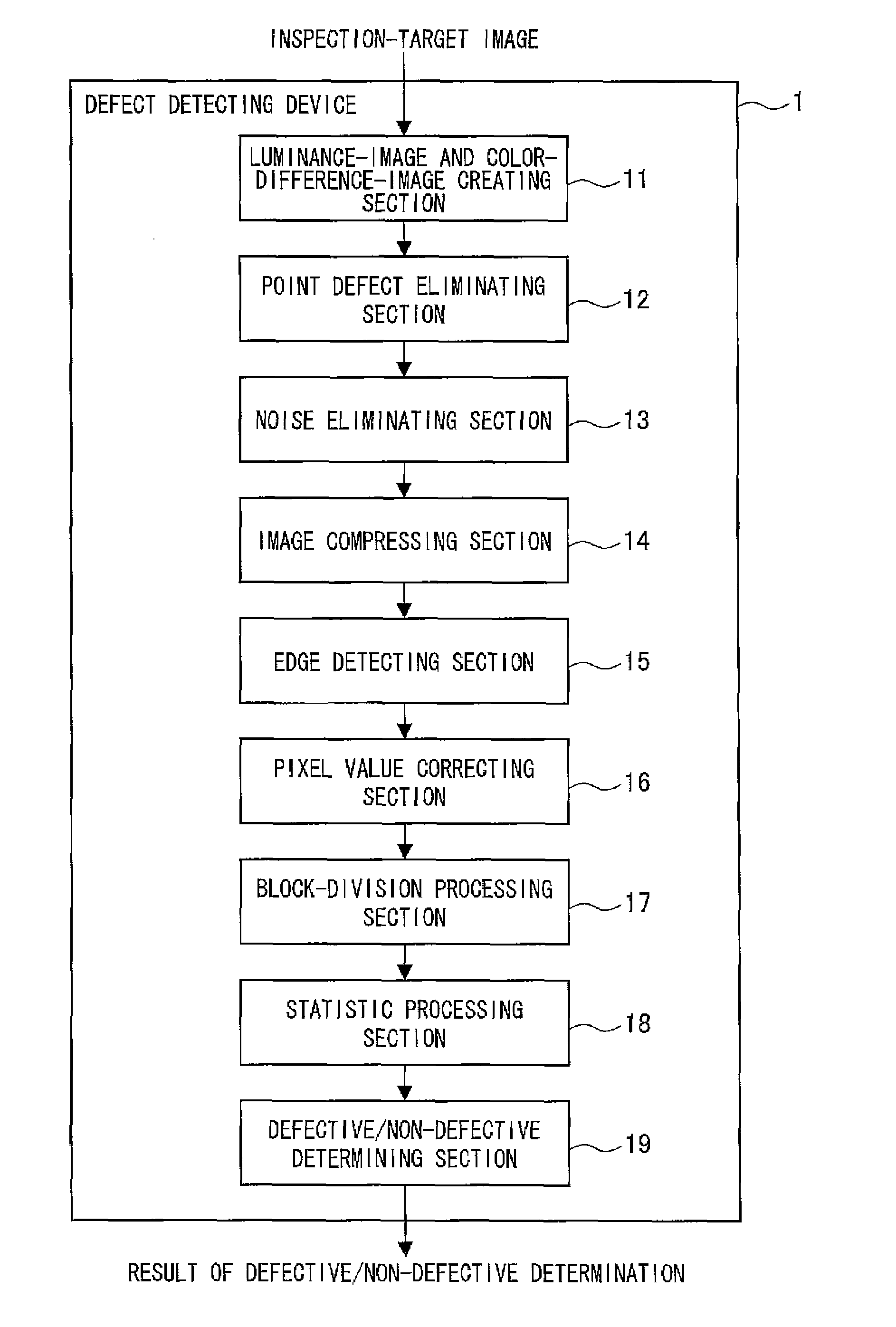
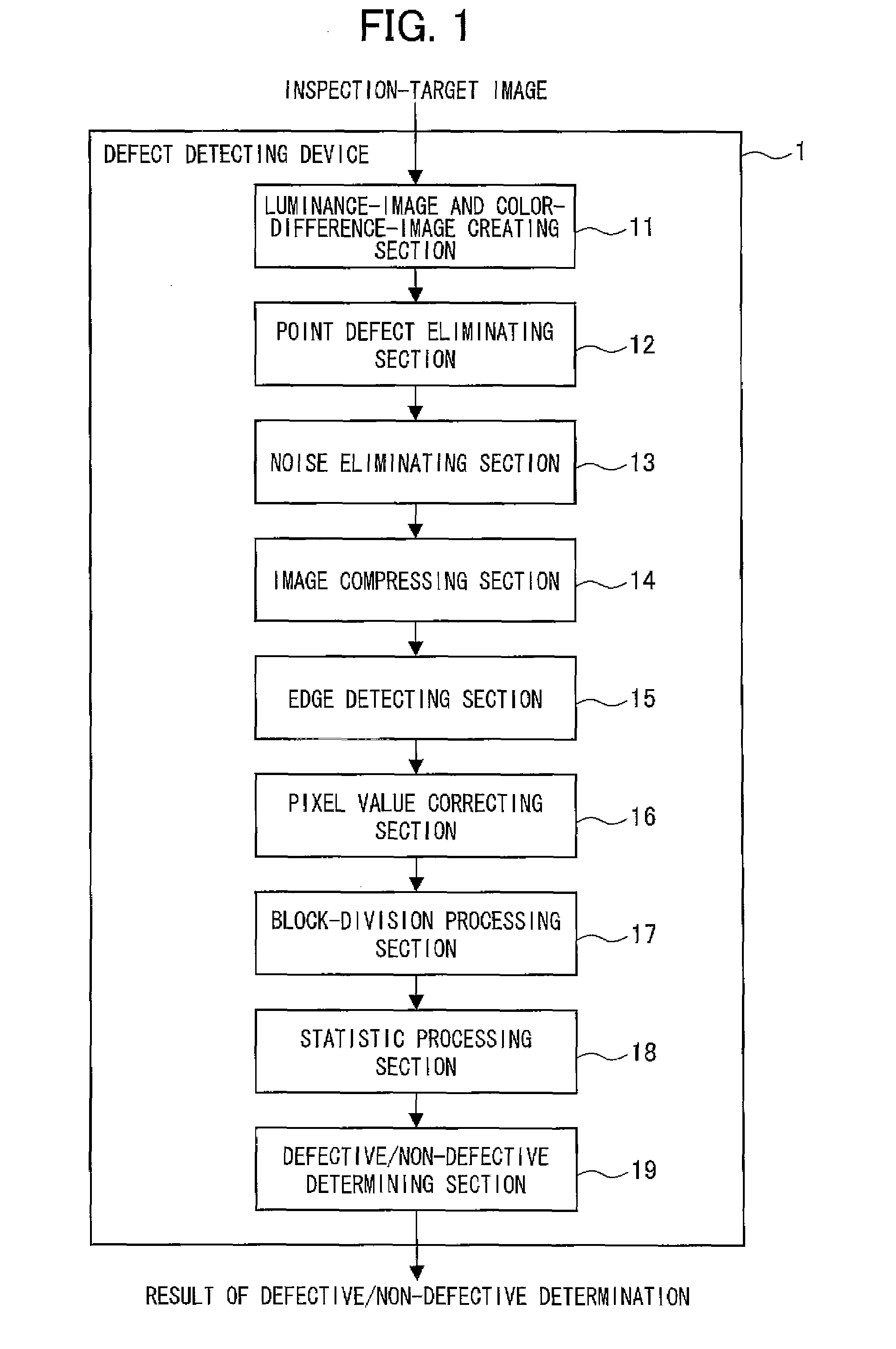
[0062]The following describes an embodiment of the present invention, with reference to FIGS. 1 to 27.

[0063]FIG. 1 is a block diagram showing a schematic configuration of a defect detecting device 1 of the present embodiment. The defect detecting device 1 includes a luminance-image and color-difference-image creating section (image creating section) 11, a point defect eliminating section 12, a noise eliminating section 13, an image compressing section 14, an edge detecting section 15, a pixel value correcting section 16, a block-division processing section 17, a statistic processing section 18 (defective-area presence determining section), and a defective / non-defective determining section 19 (defective-area presence determining section).

[0064]The luminance-image and color-difference-image creating section 11 imports an image-data image (inspection-target image), which is a target of inspection, taken by an image pickup device (not illustrated), such as ...


PUM


Abstract

A defect detecting device 1 includes a pixel value correcting section 16, a block-division processing section 17, and a defective/non-defective determining section 19. The pixel value correcting section 16 corrects a pixel value of an inspection-target image, on which detection of a defective area is to be carried out, in such a manner that the defective area of the inspection-target image is emphasized with respect to the other areas of the inspection-target image. The block-division processing section 17 divides, into plural blocks, the inspection-target image with pixel values having been corrected, and obtains a block addition value, which is a value obtained by adding pixel values of pixels present in a block, or a block mean value, which is a value obtained by dividing the block addition value by the number of pixels present in the block. The defective/non-defective determining section 19 determines whether the defective area is present or not, by carrying out statistical processing of a statistic processing section 18 to determine whether an outlier of the block addition value or an outlier of the block mean value is present or not. The foregoing realizes a defect detecting device and a defect detecting method, by which defective areas of image-sensor images are emphasized to enable accurate detection of the defective areas.

Description

[0001]This Nonprovisional application claims priority under 35 U.S.C. § 119(a) on Patent Applications No. 355595 / 2006 filed in Japan on Dec. 28, 2006, and No. 316181 / 2007 filed in Japan on Dec. 6, 2007, the entire contents of which are hereby incorporated by reference.FIELD OF THE INVENTION[0002]The present invention relates to a defect detecting device, a defect detecting method, an image sensor device, an image sensor module, a defect detecting program, and a computer-readable recording medium, by which defects are detected accurately during inspection carried out in production of image sensor devices.BACKGROUND OF THE INVENTION[0003]It is very important in quality inspection of digital images to determine whether or not there is a defective area where pixel values do not vary evenly. Especially in recent years, image sensor devices such as digital still cameras and mobiles phones with built-in cameras have been increasingly demanded. This has increased demands for image sensor de...

Claims


Application Information

Patent Timeline
IPC IPC(8): G06K9/00
CPCG06T5/20G06T7/0004G06T2207/10024G06T7/0085G06T5/002G06T5/005G06T2207/20021G06T7/13
Inventor KUCHII, TOSHIMASA
Owner SHARP KK
Why Eureka
Try Eureka