
Device threshold calibration through state dependent burnin

a technology of state dependent burnin and device threshold, which is applied in the direction of information storage, static storage, digital storage, etc., can solve the problems of limiting the performance and/or reliability of circuits that incorporate such transistors, cells and sense-amplifiers, and fatigued those devices away from their preferred states and towards, so as to avoid over-correction and reduce the effect of mismatch

Inactive Publication Date: 2008-09-11
GLOBALFOUNDRIES INC
View PDF15 Cites 27 Cited by
  • Summary
  • Abstract
  • Description
  • Claims
  • Application Information

AI Technical Summary

Benefits of technology

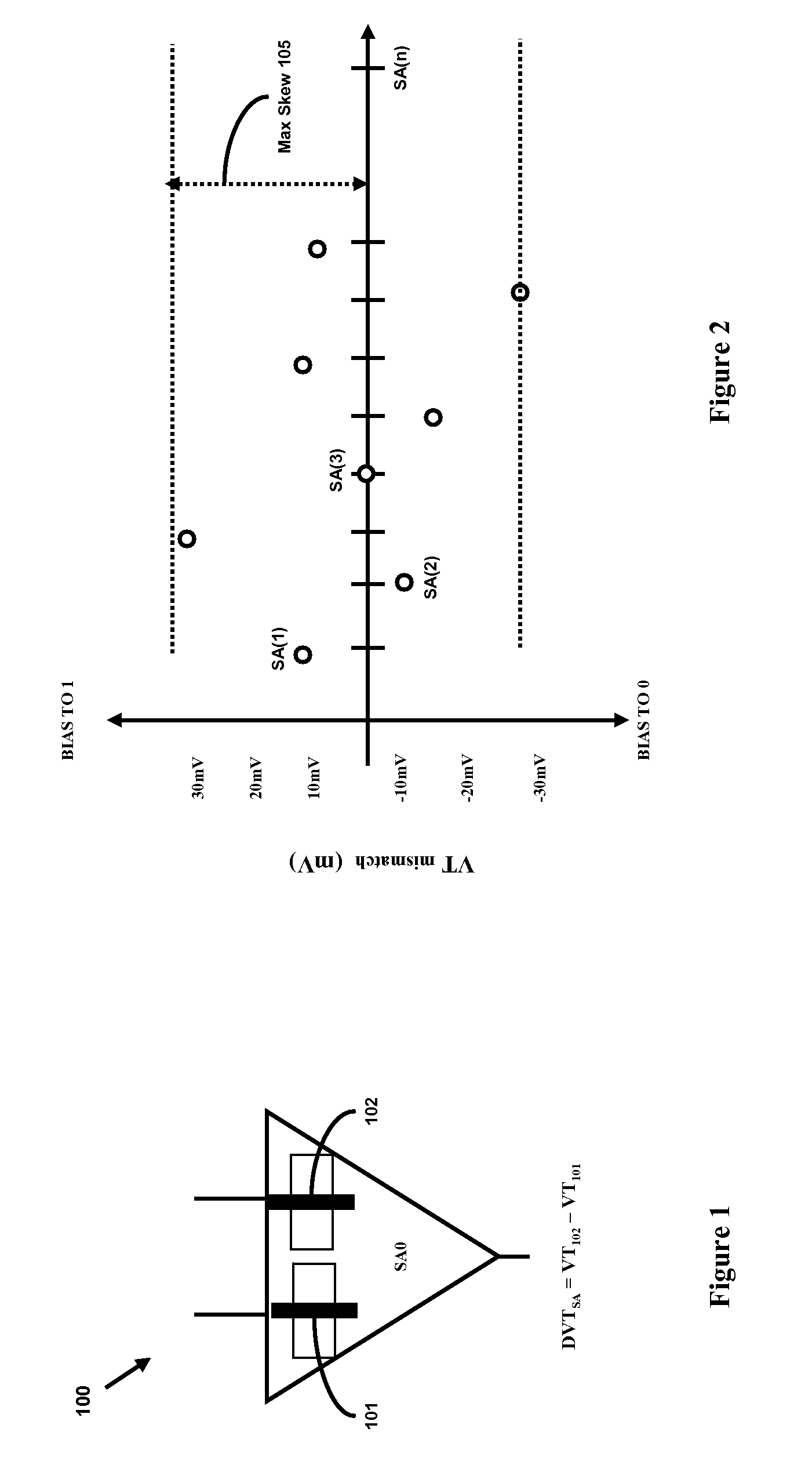
[0005]In view of the foregoing, disclosed herein are embodiments of a method for reducing and / or eliminating mismatch. The embodiments sample the bias of one or more circuit sub-components that require a balanced state (e.g., sampling the bias of the cross-coupled transistors in each memory cell and / or sense amp in a memory array) before chip burn-in, by initiating a burn-in process during which individually selected states are applied to each of the devices in the circuit. This fatigues those devices away from their preferred states and towards a balanced state (e.g., initializing each cell and sense-amplifier to unique states). The bias is periodically reassessed during the burn-in process to avoid over-correction.
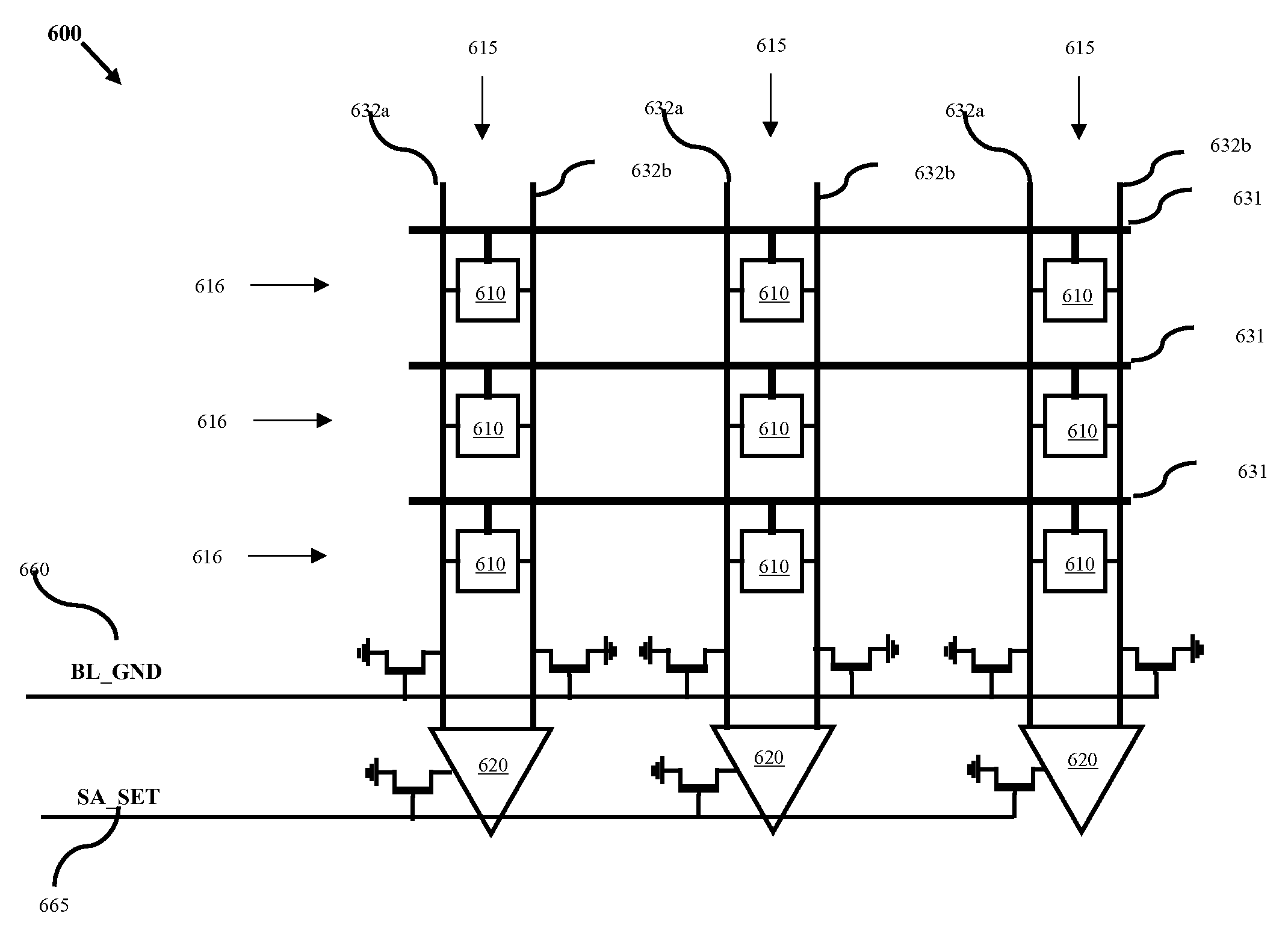
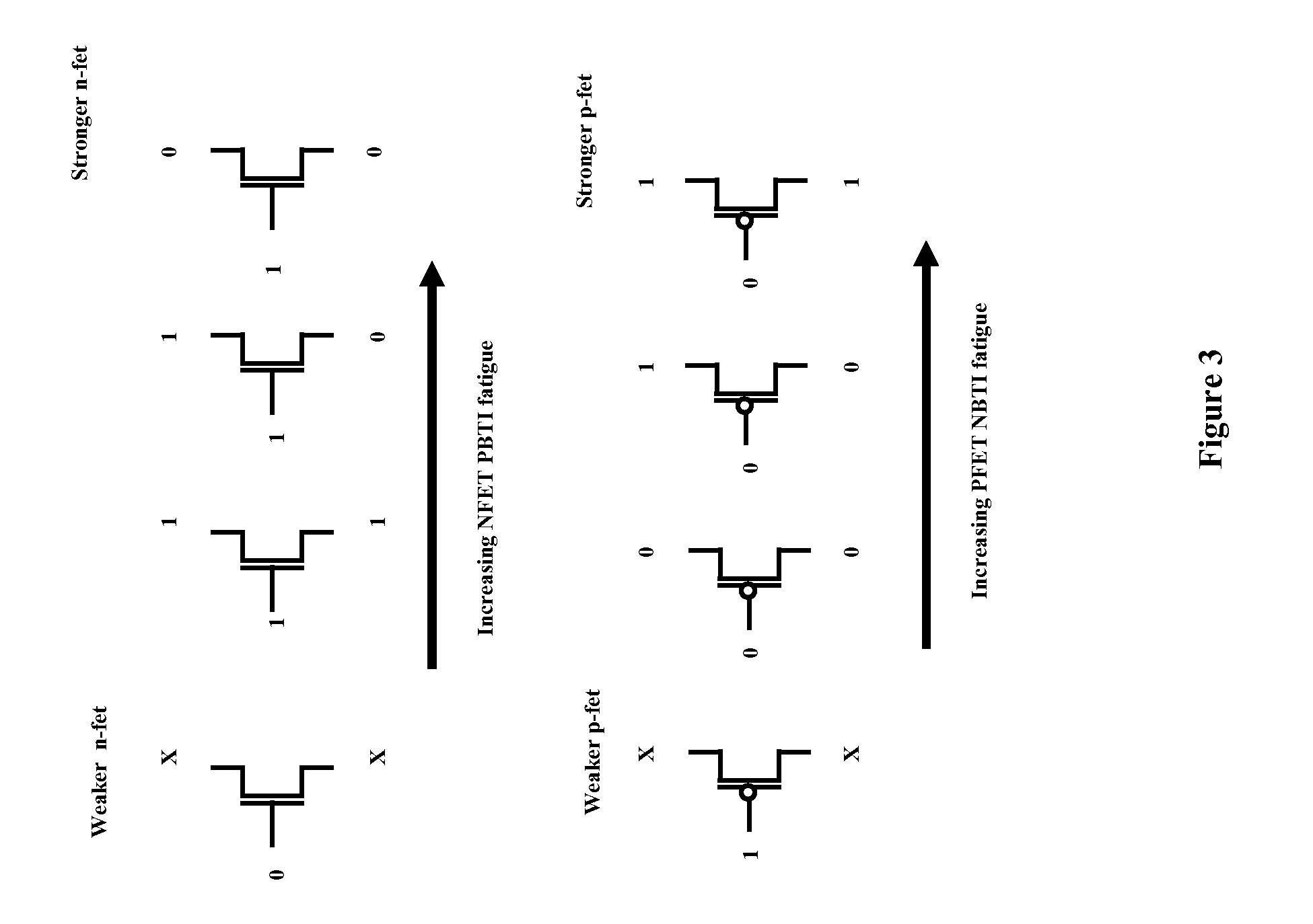
[0014]In order to individually assess and reassess the bias (i.e., the current preferred state) of each SRAM memory array sense-amplifier, the following processes can be performed. A predetermined voltage (e.g., Vdd or Vdd / 2) can be applied to all of the bit lines. Then, the SET signal of each sense-amplifier can be enabled (e.g., in succession). After the SET signal for a particular sense-amplifier is enabled, a determination can be made as to which of the cross-coupled p-type and n-type transistors in that particular sense-amplifier are stronger in order to determine the corresponding preferred state of that particular sense-amplifier. Specifically, after the SET signal is enabled, the stronger n-fet will have a low drain state and a high gate state, the weaker n-fet will have a low gate state, the stronger p-fet will have a high drain state and a low gate state, and the weaker p-fet will have a high gate state. Additionally, a combination of the opposing cross-coupled devices can act together to affect the preferred state. Then, during the burn-in process each sense-amplifier is kept in the preferred state, for example, by keeping the high gate state on the stronger n-fet, the low gate state on the weaker n-fet, the low gate state on the stronger p-fet and the high gate state on the weaker p-fet. This ensures that during the burn-in process less fatigue is applied to the weaker n-fet and the weaker p-fet and more fatigue is applied to the stronger n-fet and the stronger p-fet. Applying more fatigue to the stronger transistors during burn-in weakens them and, thereby, reduces threshold voltage differences between the opposing sides of the cross-coupled transistors.
[0015]In order to individually assess and reassess the bias (i.e., the current preferred state) of each of SRAM memory cell, the following processes can be performed. First, the word lines are pulsed sequentially (i.e., word line to word line) at a high state. Meanwhile, all of the bit lines are kept at a predetermined voltage (e.g., ground or Vdd / 2). Then, a determination is made as to which of the cross-coupled p-type and n-type transistors in each of the memory cells are stronger and which are weaker so as to determine the corresponding preferred state. Specifically, after a word line connected to a particular memory cell is pulsed, the stronger n-fet in that memory cell will have a low drain state and a high gate state, the weaker n-fet will have a low gate state, the stronger p-fet will have a high drain state and a low gate state, and the weaker p-fet will have a high gate state. As with the sense-amplifiers discussed above, each one of the memory cells is kept in the preferred state during the burn-in by keeping the high gate state on the stronger n-fet, the low gate state on the weaker n-fet, the low gate state on the stronger p-fet and the high gate state on the weaker p-fet. This ensures that during the burn-in process less fatigue is applied to the weaker n-fet and the weaker p-fet and more fatigue is applied to the stronger n-fet and the stronger p-fet. Again, applying more fatigue to the stronger transistors during burn-in weakens them and, thereby, balances the transistors.

Problems solved by technology

These variations can limit the performance and / or reliability of circuits that incorporate such transistors.
Mismatches between the cross-coupled transistors (i.e., variations in threshold voltage, length, width, and other device parameters between the cross-coupled transistors) in both the individual memory cells and the sense-amplifiers can produce incorrect results.
This fatigues those devices away from their preferred states and towards a balanced state (e.g., initializing each cell and sense-amplifier to unique states).
For example, for a latch-type device, such as a memory cell or a sense-amplifier, keeping the device in the preferred state, during a burn-in process will fatigue the device towards a balanced state.
Again, applying more fatigue to the stronger transistors during burn-in weakens them and, thereby, balances the transistors.

Method used


Image

  • Device threshold calibration through state dependent burnin
  • Device threshold calibration through state dependent burnin
  • Device threshold calibration through state dependent burnin

Examples


Embodiment Construction

[0028]The embodiments of the invention and the various features and advantageous details thereof are explained more fully with reference to the non-limiting embodiments that are illustrated in the accompanying drawings and detailed in the following description. It should be noted that the features illustrated in the drawings are not necessarily drawn to scale. Descriptions of well-known components and processing techniques are omitted so as to not unnecessarily obscure the embodiments of the invention. The examples used herein are intended merely to facilitate an understanding of ways in which the embodiments of the invention may be practiced and to further enable those of skill in the art to practice the embodiments of the invention. Accordingly, the examples should not be construed as limiting the scope of the embodiments of the invention.

[0029]As mentioned above, as technology scales to sub-micron geometries Random Device Variation (RDV) is becoming more prominent. That is, as in...


PUM


Abstract

Disclosed are embodiments of a method for reducing and / or eliminating mismatch. The embodiments sample the bias of one or more circuit sub-components that require a balanced state (e.g., sampling the bias of the cross-coupled transistors in each memory cell and / or sense amp in a memory array) before chip burn-in, by initiating a burn-in process during which an individually selected state is applied to each of the devices in the circuit. This fatigues the devices away from their preferred states and towards a balanced state. The bias is periodically reassessed during the burn-in process to avoid over-correction. By using this method both memory cell and sense-amplifier mismatch can be reduced in memory arrays, resulting in smaller timing uncertainty and therefore faster memories.

Description

BACKGROUND[0001]1. Field of the Invention[0002]The embodiments of the invention generally relate to devices having cross-coupled latches that require a balanced state. The balanced state being defined by an equal probability of the latch resolving to a “1” or a “0” when the cross-coupled data nodes are initialized to the same voltage. More particularly, this invention relates to a method of compensating for process-induced Random Device Variation (RDV). In addition, this method can also be applied to other threshold sensitive circuitry that can be affected by RDV. Sense-amplifier circuitry that requires matching characteristics between commonly enabled sense-amplifiers can also be calibrated using this approach.[0003]2. Description of the Related Art[0004]As technology scales to sub-micron geometries, Random Device Variation (RDV) is becoming more prominent. That is, as individual devices, such as field effect transistors (FETs), continue to shrink in size (e.g., from approximately ...

Claims


Application Information

Patent Timeline
Patent Type & Authority Applications(United States)
IPC IPC(8): G11C7/00
CPCG11C11/41G11C29/50G11C29/028
Inventor ARSOVSKI, IGORPILO, HAROLDZIEGERHOFER, MICHAEL A.
Owner GLOBALFOUNDRIES INC
Learn More