
Liquid crystal display and manufacturing method thereof

a technology of liquid crystal display and manufacturing method, which is applied in the manufacture of electrode systems, electric discharge tubes/lamps, instruments, etc., can solve the problems of ineffective cleaning execution, and achieve the effect of suppressing the degradation of yield caused by corrosion around the terminal and high-reliability liquid crystal display

Inactive Publication Date: 2008-09-18
MITSUBISHI ELECTRIC CORP
View PDF4 Cites 1 Cited by
  • Summary
  • Abstract
  • Description
  • Claims
  • Application Information

AI Technical Summary

Benefits of technology

[0007]An aspect of the present invention has been made in view of the above mentioned circumstances and provides a high-yield and high-reliability liquid crystal display and a manufacturing method thereof.
[0009]According to the invention, yield degradation caused by corrosion around the terminal can be suppressed and a highly reliable liquid crystal display can be provided easily.

Problems solved by technology

To use the method of JP-A-5-232422 as described above, it is effective for preventing corrosion at the cleaning time before cell cutting, but is not effective for cleaning executed after injecting liquid crystal or after injection hole sealing performed after cell cutting; liquid for cleaning enters an area sandwiched between the substrate and the seal and terminal corrosion occurs in a terminal drawing wiring part in the proximity of the seal.

Method used


Image

  • Liquid crystal display and manufacturing method thereof
  • Liquid crystal display and manufacturing method thereof
  • Liquid crystal display and manufacturing method thereof

Examples


first embodiment

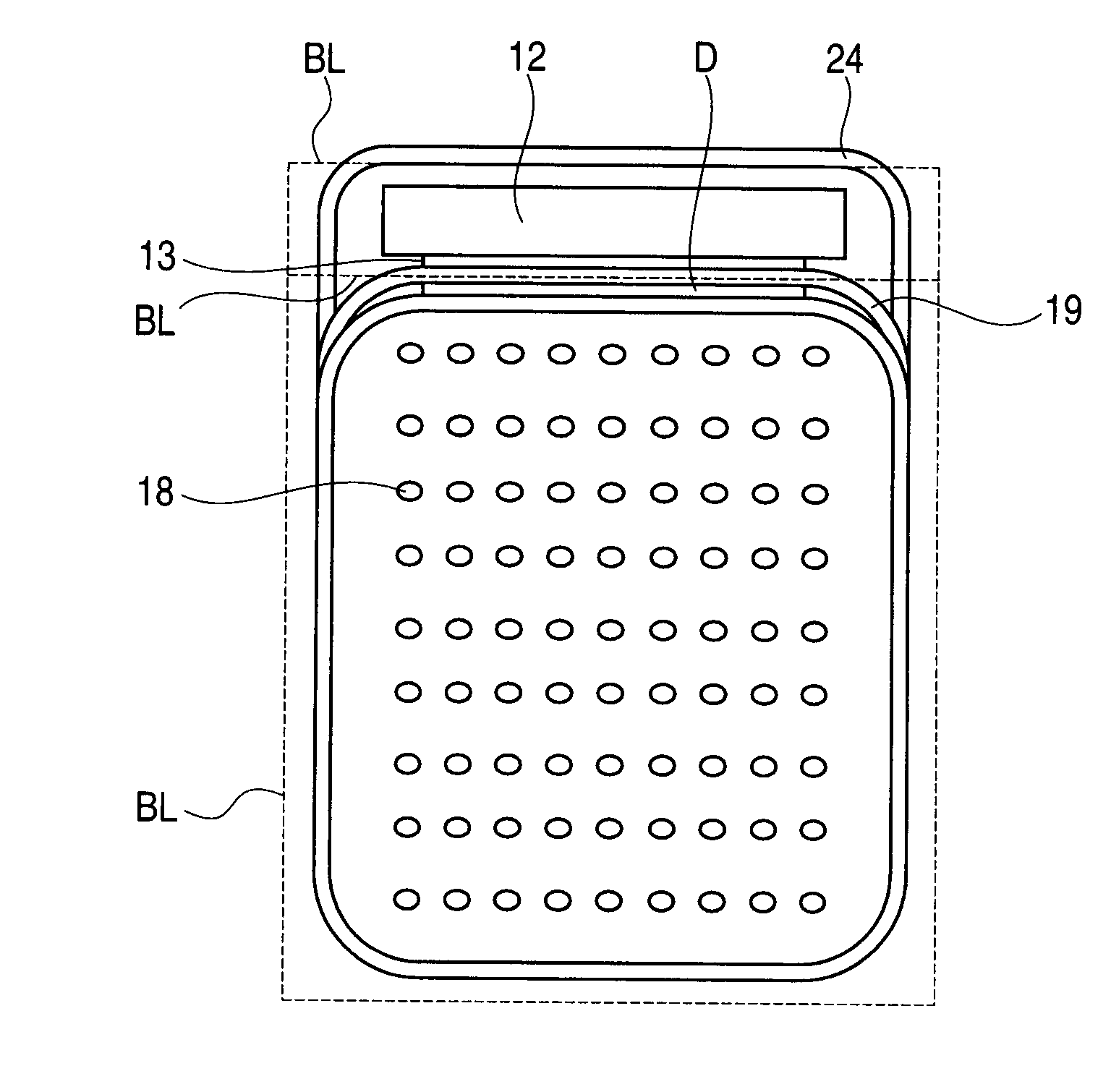
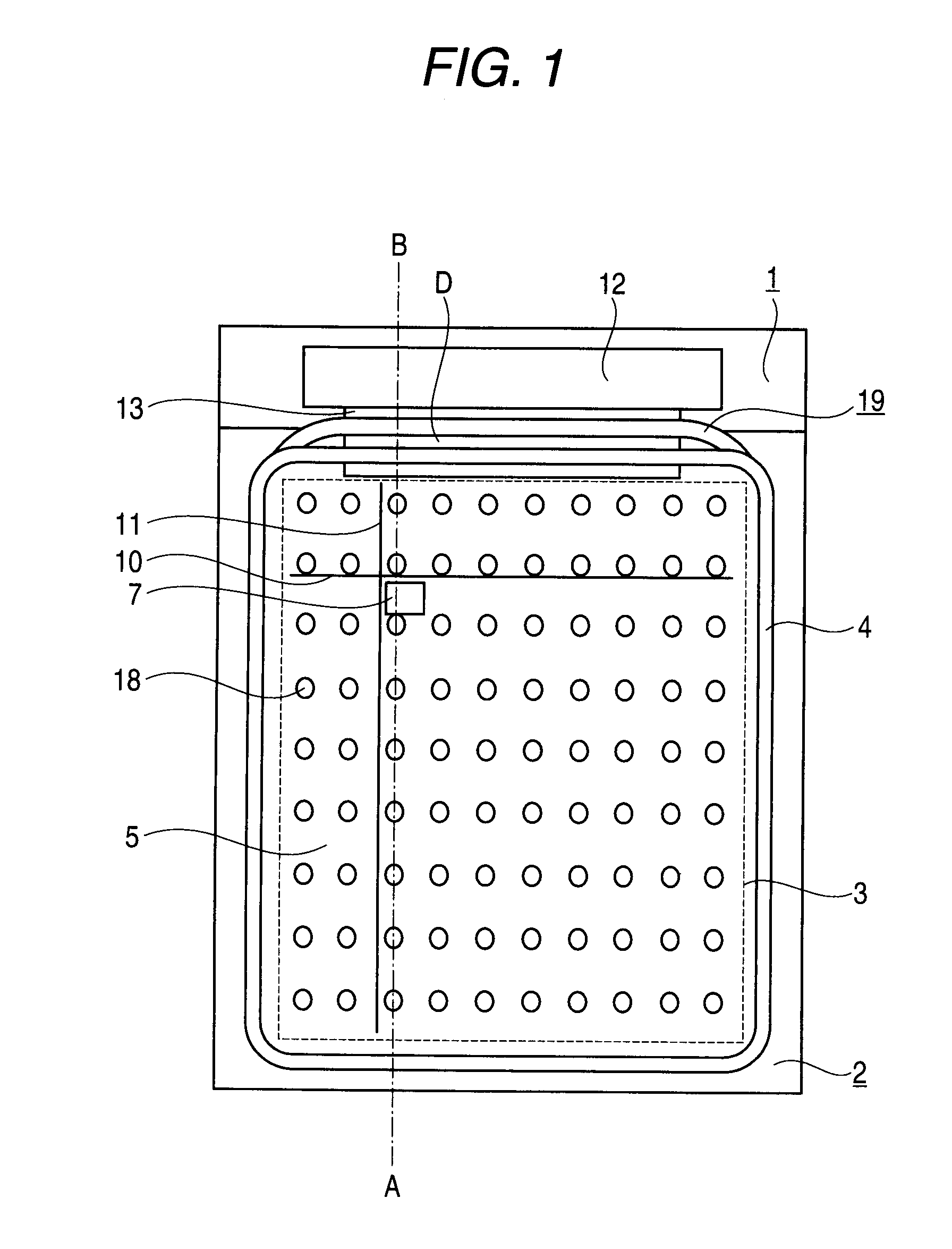
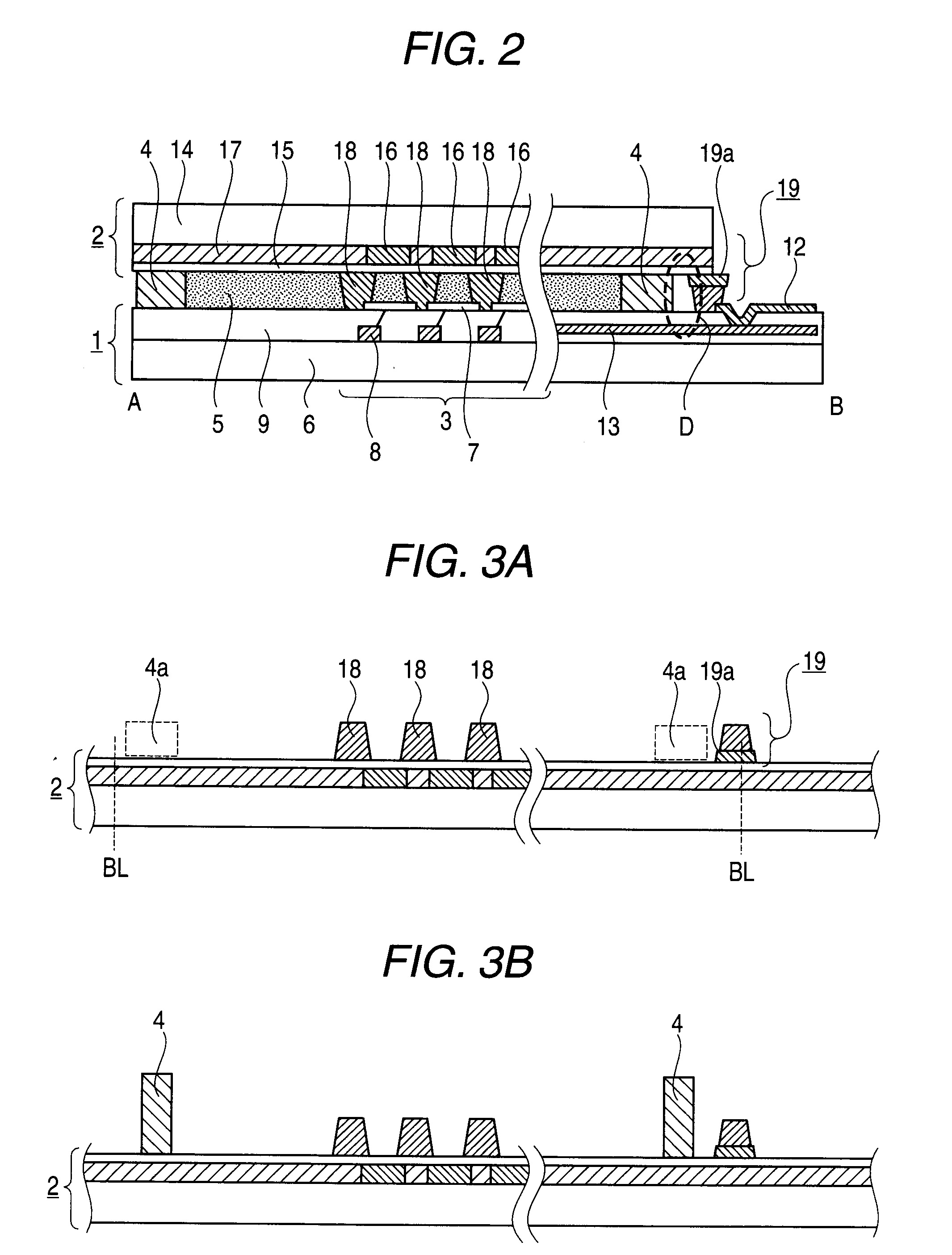
[0021]A liquid crystal display of a first embodiment of the invention will be discussed with FIGS. 1 and 2. FIG. 1 is a plan view to show the whole liquid crystal display and FIG. 2 is a sectional view taken on dashed line A-B in FIG. 1. The figures are schematic and do not reflect exact dimensions of shown components, etc. Throughout the Specification, components identical with those previously described with reference to the accompanying drawings are denoted by the same reference numerals and will not be discussed again. This is also applied in other figures.

[0022]The liquid crystal display of the first embodiment includes a terminal substrate 1, a color filter substrate 2 opposed to the terminal substrate 1, a seal 4 formed so as to surround a display area 3 for displaying an image in the peripheral portion of the color filter substrate 2, and liquid crystal 5 filled into the space between the terminal substrate 1 and the color filter substrate 2, surrounded by the seal 4, as sho...

second embodiment

[0038]In the first embodiment, the columnar spacers 18 are formed on the color filter substrate 2 and accordingly, the protective wall 19 is also formed on the color filter substrate 2. In contrast, a second embodiment of the invention is a modified example of changing the placement in the first embodiment so as to form the columnar spacers 18 and the protective wall 19 on the terminal substrate 1. The second embodiment will be discussed.

[0039]To begin with, the configuration of a liquid crystal display of the second embodiment will be discussed with a sectional view of FIG. 5. The second embodiment differs from the first embodiment in that columnar spacers 18 and a protective wall 19 formed of only the same material as the columnar spacers 18 are formed so that they are fixedly secured to a terminal substrate 1. The configuration other than the change is similar to that of the first embodiment previously described with reference to FIG. 2 and therefore will not be discussed again i...

third embodiment

[0044]In the second embodiment, the columnar spacers 18 and the protective wall 19 are formed of the same material on the terminal substrate 1 at the same time. In contrast, a third embodiment of the invention is a modified example of changing the second embodiment so as to place the columnar spacers 18 so that it is fixedly secured to the color filter substrate 2 as in the first embodiment and form the columnar spacers 18 and the protective wall separately. The third embodiment will be discussed.

[0045]A manufacturing method of a liquid crystal display of the third embodiment will be discussed with FIG. 7. FIG. 7 corresponds to FIG. 6 of a schematic representation of the manufacturing method in the second embodiment. As shown in FIG. 7, in the third embodiment, unlike the second embodiment, columnar spacers 18 are formed on a color filter substrate 2 and a protective wall 21 is formed of a sealing compound made of uncured resign independently of the columnar spacers 18 on the termin...


PUM

PropertyMeasurementUnit
display areaaaaaaaaaaa
areaaaaaaaaaaa
conductiveaaaaaaaaaa

Abstract

A liquid crystal display includes a terminal substrate, an opposed substrate, a seal member and a protective wall. The terminal substrate includes: a display area which displays an image, a terminal which inputs an external signal to a wiring in the display area, and a connection conductor which electrically connects the wiring in the display area and the terminal. The opposed substrate includes a conductive film on a surface thereof. The seal member surrounds the display area and through which the terminal substrate and opposed substrate are attached with each other while being opposed with each other. The protective wall surrounds a proximity portion of the connection conductor and the conductive film outside of an area surrounded by the seal member, together with the seal member to isolate and protect the proximity portion from an outside.

Description

CROSS-REFERENCE TO RELATED APPLICATIONS[0001]This application is based upon and claims the benefit of priority from Japanese Patent Application No. 2007-064910, filed Mar. 14, 2007, the entire contents of which are incorporated herein by reference.BACKGROUND OF THE INVENTION[0002]1. Field of the Invention[0003]This invention relates to a liquid crystal display and a manufacturing method thereof.[0004]2. Description of the Related Art[0005]In a manufacturing method of a liquid crystal display, when cells are cut or after liquid crystal is injected into the cut cells, a step of cleaning each cell is executed. A liquid for the cleaning may enter the cell or corrosion may occur in a terminal portion, etc., because of the remaining liquid. JP-A-5-232422 discloses a technique to surround the outer peripheral portion of a substrate with a seal, thereby preventing liquid entry at the cleaning time when a cut scratch at cutting cells is formed.SUMMARY OF THE INVENTION[0006]To use the method ...

Claims


Application Information

Patent Timeline
Patent Type & Authority Applications(United States)
IPC IPC(8): G02F1/1339G02F1/13
CPCG02F1/1345G02F1/1339
Inventor SOMA, YUKI
Owner MITSUBISHI ELECTRIC CORP
Learn More