

Sensor element and sensor assembly provided with a casing
a sensor and casing technology, applied in the field of sensor elements, can solve the problems of sensor measurement signal errors, sensor stress and external stress, etc., and achieve the effect of less sensitive to stress and forces
- Summary
- Abstract
- Description
- Claims
- Application Information
AI Technical Summary
Benefits of technology
Problems solved by technology
Method used
Image

Examples
Embodiment Construction
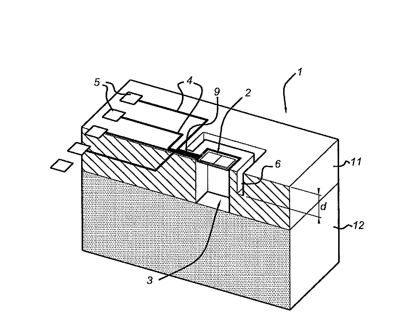
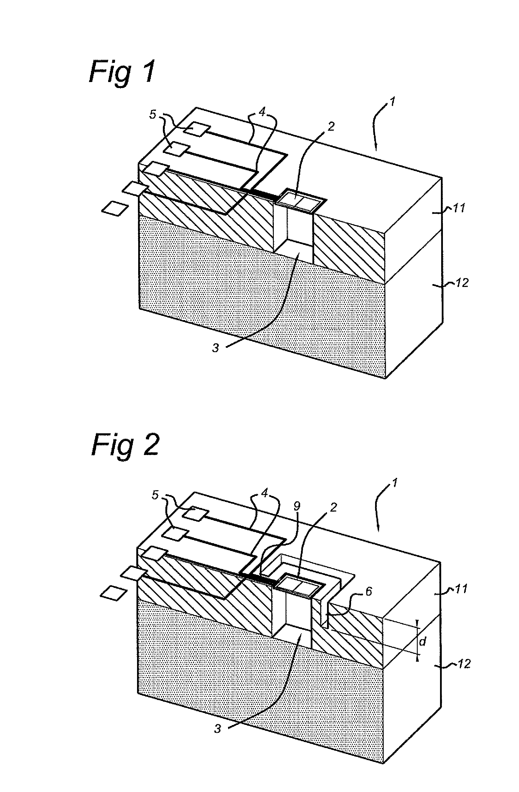
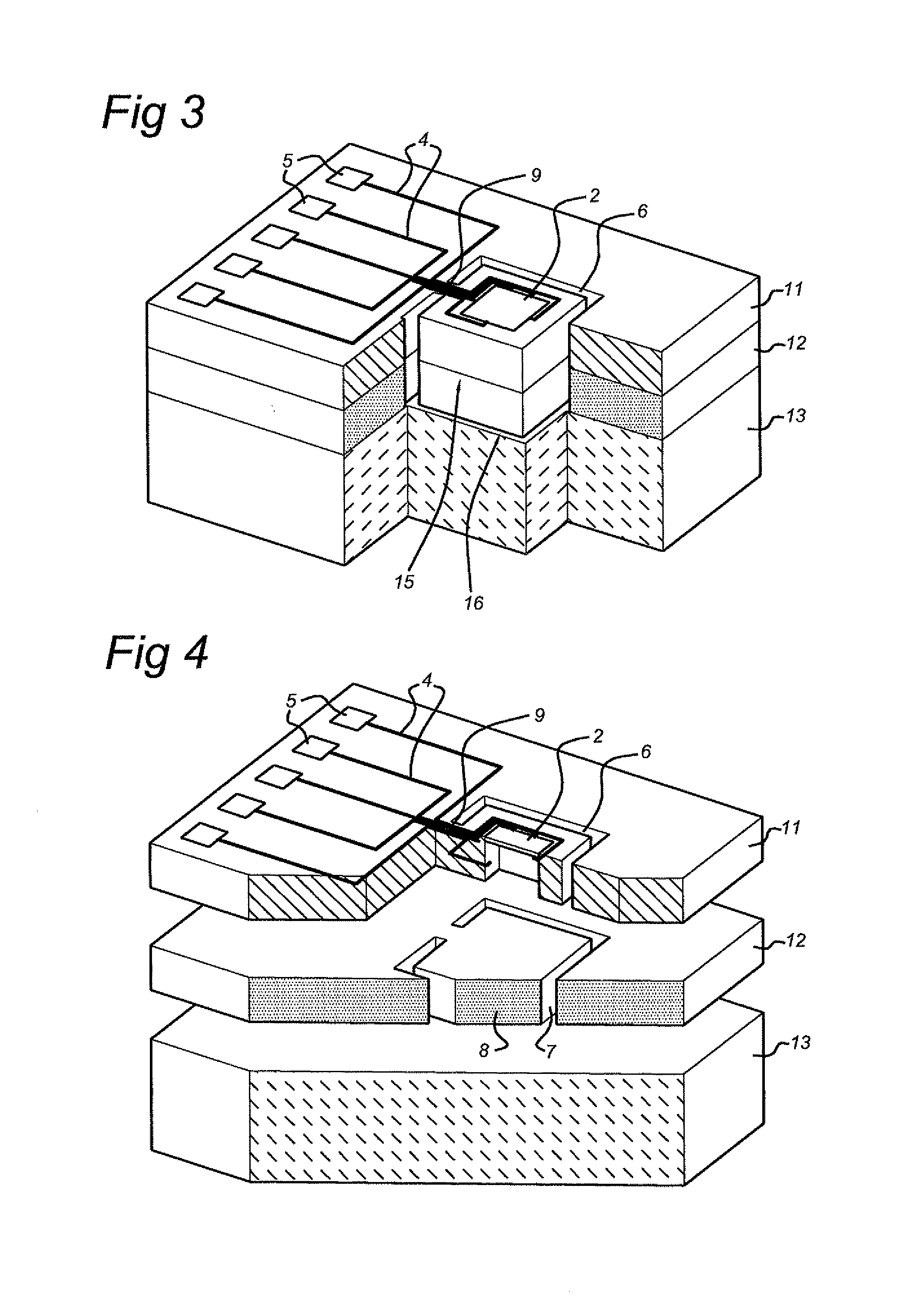
[0024]FIG. 1 shows a cross-sectional view in perspective of a (semiconductor) sensor element 1 which is produced according to known techniques. The sensor element 1 is composed of a first (active) substrate layer 11, for example made of semiconductor material, in which conductive tracks 4 are provided on the upper side of the first substrate layer 11, which electrically connect a sensitive sensor portion 2 to connection regions 5. During the manufacturing process of an entire chip, lead wires are wire-stitched, welded or soldered onto the connection regions 5. In the illustrated embodiment, the sensitive sensor portion 2 is a membrane on top of a cavity or chamber 3. The membrane 2 is, for example, provided with a number of strain gauges in a Wheatstone bridge configuration, resulting in a pressure sensor. In the illustrated embodiment, the cavity 3 is closed off by a second substrate layer 12, which is hermetically connected to the first substrate layer 11. This makes the sensor el...
PUM
 Abstract
Description
Claims
Application Information