
Integrated circuit having resistor between beol interconnect and feol structure and related method

a technology of integrated circuits and resistors, which is applied in the direction of electrical equipment, semiconductor devices, semiconductor/solid-state device details, etc., can solve the problems of difficult to obtain a common process for these two types of beol contacts, and achieve the effect of low topography

Inactive Publication Date: 2008-10-02
ALSEPHINA INNOVATIONS INC
View PDF19 Cites 55 Cited by
  • Summary
  • Abstract
  • Description
  • Claims
  • Application Information

AI Technical Summary

Benefits of technology

"The patent text describes an integrated circuit and a method of fabricating it that includes a back-end-of-the-line (BEOL) thin film resistor. This structure helps to achieve lower topography by avoiding the necessity of forming contacts with differing heights or contacts over varying topography. The invention provides an integrated circuit with a first resistor between a BEOL interconnect and a front-end-of-the-line (FEOL) structure, and a method of fabricating it that includes a first resistor and a first metal layer of the BEOL interconnect. The technical effects of this invention include improved performance and reliability of the integrated circuit."

Problems solved by technology

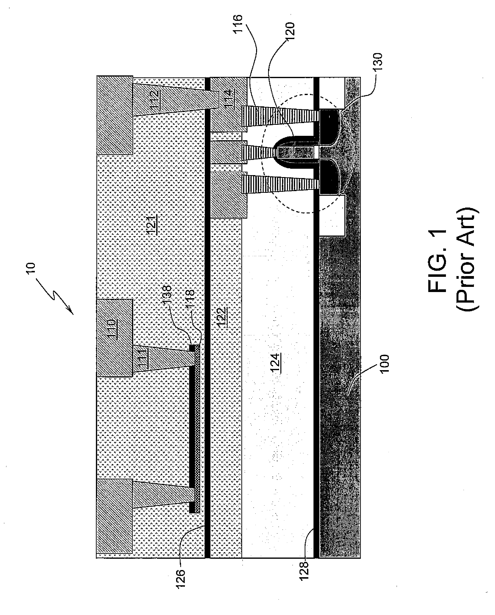
It is difficult to obtain a common process for these two types of BEOL contacts, especially if the height difference between BEOL contact 111 and BEOL contact 112 is large.

Method used


Image

  • Integrated circuit having resistor between beol interconnect and feol structure and related method
  • Integrated circuit having resistor between beol interconnect and feol structure and related method
  • Integrated circuit having resistor between beol interconnect and feol structure and related method

Examples


Embodiment Construction

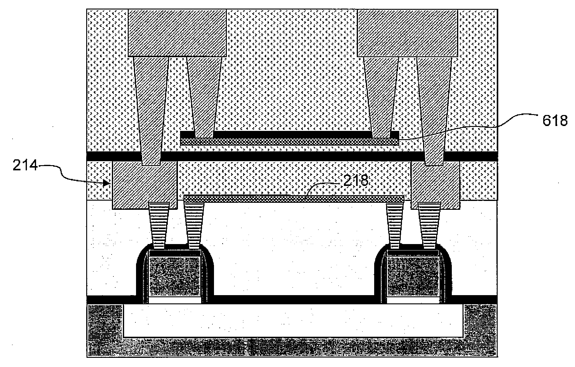
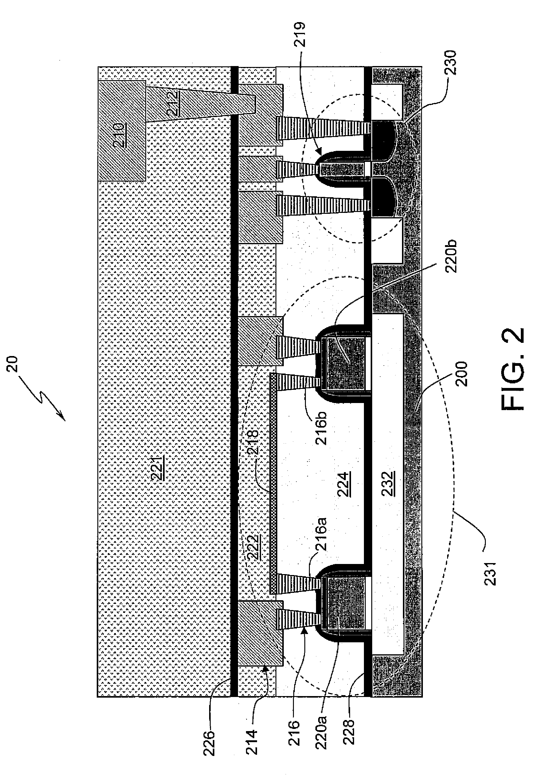
[0015]Various embodiments are depicted in the drawings in FIGS. 2-7. The figures illustrate the different aspects of connecting a multiple thin film resistor 218, hereinafter resistor / first resistor 218, incorporated into an integrated circuit (IC) 20 below a first metal layer 214 of a back-end-of-the-line (BEOL) fabrication process.

[0016]FIG. 2 illustrates an integrated circuit (IC) 20 where multiple layers of interconnect fabricated by the BEOL process are above a structure fabricated with a front-end-of-the-line (FEOL) process. The BEOL portion of the IC begins with a first metal layer 214 while the FEOL portion of the IC ends at the layer prior to first metal layer 214. The FEOL portion is fabricated on a substrate 200 and includes devices 230 and 231 which may be connected by a wiring path (not shown). Such devices 230, 231 usually include one or more polysilicon members 219, 220a, 220b. For example, device 230 may be a transistor where polysilicon member 219 may be a gate; and...


PUM


Abstract

Integrated circuits (IC) and a method of fabricating an IC, where the structure of the IC incorporates a back-end-of-the-line (BEOL) thin film resistor below a first metal layer to achieve lower topography are disclosed. The resistor directly contacts any one of: a contact metal in the front-end-of-the-line (FEOL) structure; first metal layer in the BEOL interconnect; or the combination thereof, to avoid the necessity of forming contacts with differing heights or contacts over varying topography.

Description

BACKGROUND[0001]1. Technical Field[0002]The disclosure relates to integrated circuit (IC) chip fabrication, and more particularly, to integrated circuits (IC) with resistors of lower topography and methods of forming a resistor below the first metal layer of a back-end-of-the-line (BEOL) interconnect structure.[0003]2. Related Art[0004]In the current state of the art, thin film resistors in integrated circuits are typically incorporated as part of the back-end-of-the-line (BEOL) interconnect. To establish connectivity between a device in the front-end-of-the-line (FEOL) to a thin film resistor in the BEOL, a wiring path traverses a myriad of connectivity points between many metal layers. The usual wiring path traverses a contact layer; a first metal layer; contacts that connect the metal layers; subsequent metal layers above the first metal layer; multiple thin film resistors; and, in reverse, to the first metal layer and then the contact layer. A simplified example of a typical int...

Claims


Application Information

Patent Timeline
Patent Type & Authority Applications(United States)
IPC IPC(8): H01L29/00H01L21/20
CPCH01L21/76895H01L23/5228H01L2924/0002H01L2924/00
Inventor CHINTHAKINDI, ANIL K.MCGAHAY, VINCENT J.
Owner ALSEPHINA INNOVATIONS INC
Learn More