
Micromechanical system

a micro-mechanical system and micro-mechanical technology, applied in the field of micro-mechanical systems, can solve the problems of marked decline in the mechanical stability of connecting elements, affecting the manufacturing of high-resolution structures,

Inactive Publication Date: 2011-03-24
ROBERT BOSCH GMBH
View PDF4 Cites 0 Cited by
  • Summary
  • Abstract
  • Description
  • Claims
  • Application Information

AI Technical Summary

Benefits of technology

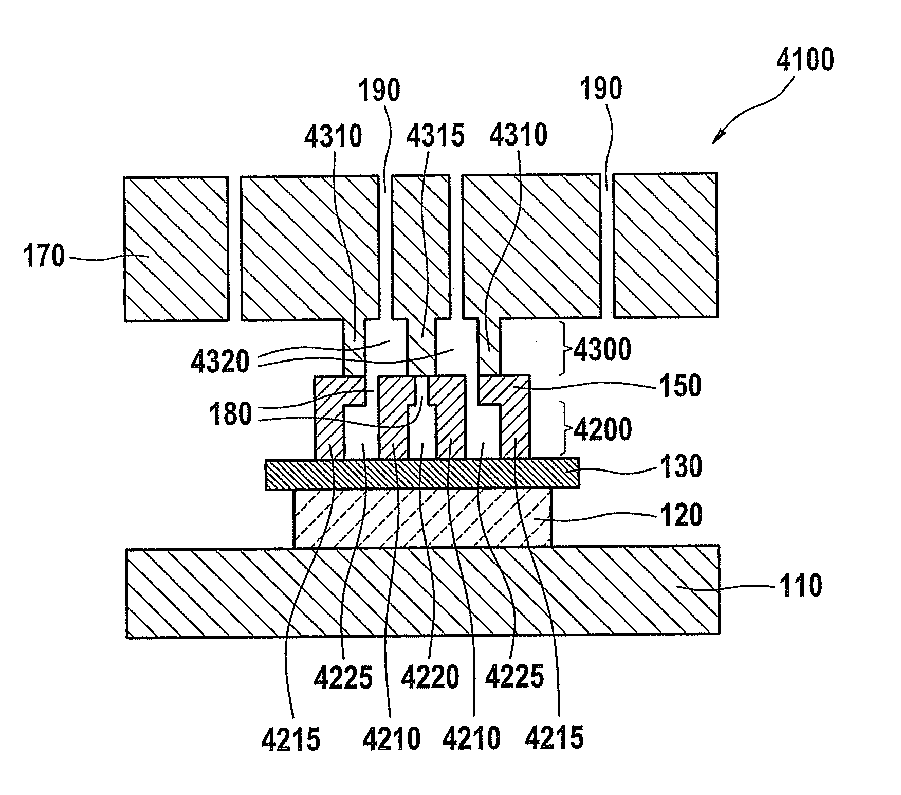
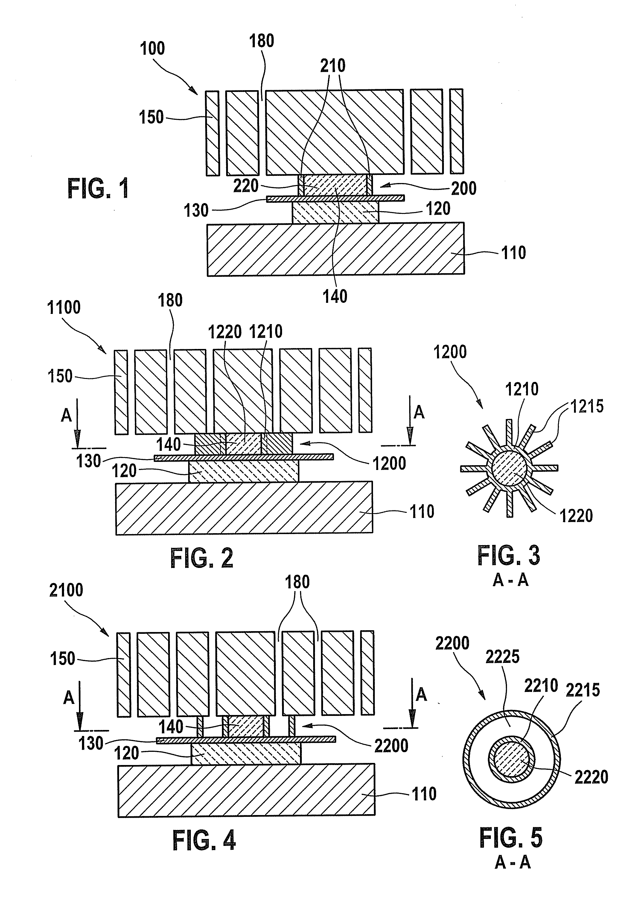
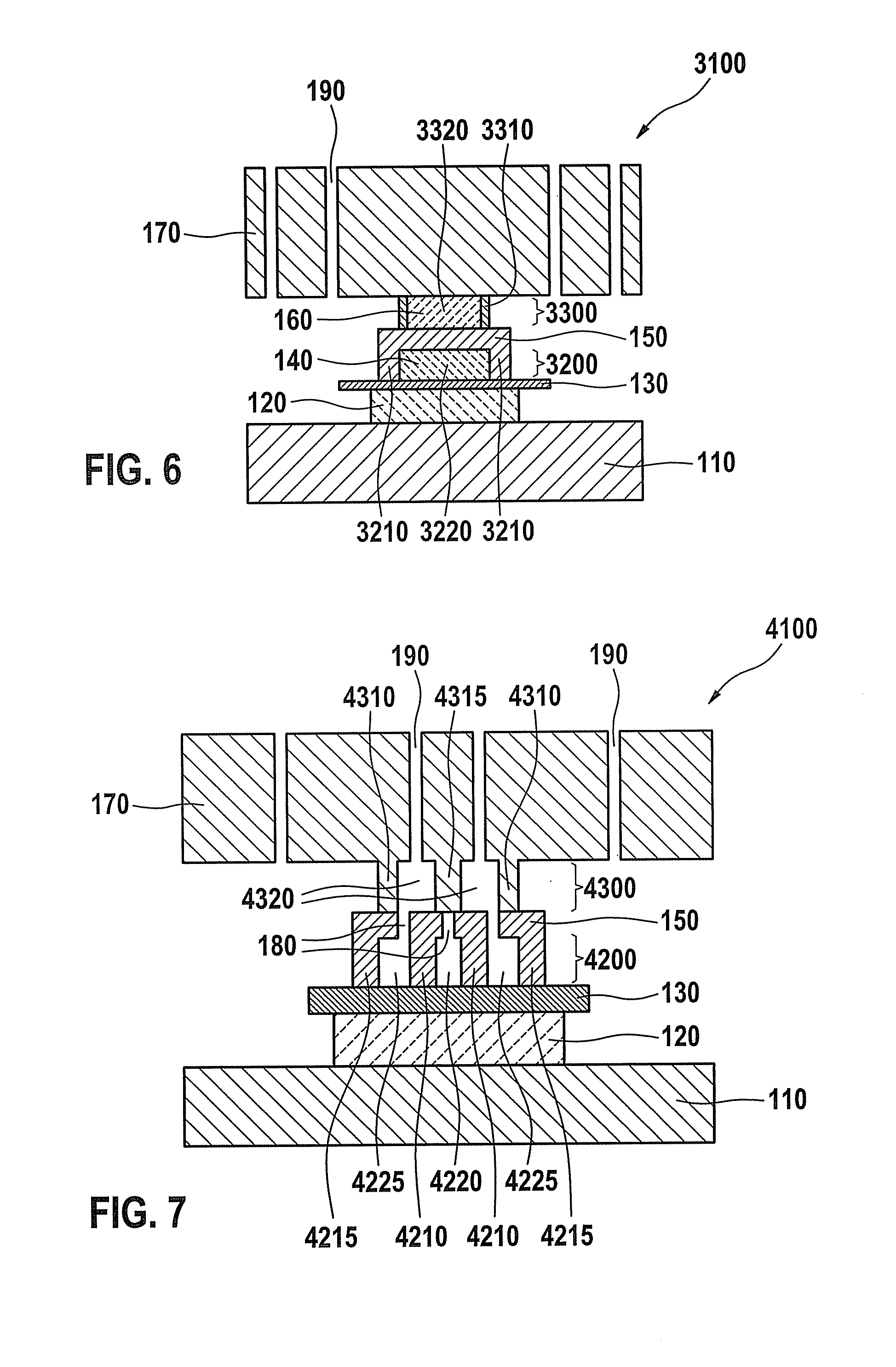
[0004]A micromechanical system according to the present invention includes a substrate, a first conductive layer situated above the substrate and a second conductive layer situated above the first conductive layer. The first conductive layer and the second conductive layer are conductively interconnected by a first connecting element. The first connecting element has a first conductive edge which surrounds a first nonconductive region. The second conductive layer advantageously has only a low topography over the connecting element. The connecting element nevertheless has a very high mechanical stability. One particular advantage is that mechanical elastic and torsion properties of the connecting element are adjustable by varying the volume and the material composition of the nonconductive region.
[0007]In one refinement, the first conductive edge surrounds another conductive region extending from the first conductive layer to the second conductive layer. This advantageously makes it possible to increase the conductivity of the connecting element. Furthermore, the further conductive region may also border a nonconductive region. Such a chamber structure makes it possible to design the mechanical properties of the connecting element as desired.
[0011]A method according to the present invention for manufacturing a micromechanical system has method steps for providing a substrate with a first conductive layer, for depositing and structuring a second insulating layer, creating, in the second insulating layer, a trench extending from the surface of the second insulating layer to the first conductive layer and bordering a section of the second insulating layer, for depositing a second conductive layer and for removing a portion of the second insulating layer. This method advantageously allows the manufacture of a mechanically stable connection between the first and second conductive layers and therefore creates only minor differences in height in the surface of the second conductive layer. Another advantage is that the mechanical properties of the conductive connection between the conductive layers are adaptable to the particular requirements.
[0013]It is also expedient if at least one through opening is created in the second conductive layer and if the second part of the second insulating layer is removed by an etching process. The region of the second insulating layer bordered by the resulting conductive edge between the first and second conductive layers may advantageously be either removed or retained. This allows the mechanical properties of the connecting element to be varied.

Problems solved by technology

This results in an irregular elevation profile (topography) on the surface of the newly applied conductive layer, thus hindering the manufacturing of high-resolution structures.
However, there is a marked decline in the mechanical stability of the connecting elements at the same time.

Method used


Image

  • Micromechanical system
  • Micromechanical system
  • Micromechanical system

Examples


Embodiment Construction

[0021]FIG. 1 shows a section through a layer structure of a micromechanical system 100 in a highly schematic diagram. Micromechanical system 100 may be part of a micromechanical sensor structure such as an acceleration sensor or a yaw sensor, for example. Micromechanical system 100 includes a substrate 110, which functions as the carrier. Substrate 110 may be a silicon substrate, for example. A first insulating layer 120 is provided on the surface of substrate 110. First insulating layer 120 is preferably embodied as a sacrificial layer and is made of a silicon oxide, for example. A first conductive layer 130 is situated on first insulating layer 120. First conductive layer 130 may be a buried polysilicon layer, for example. For example, conductor paths may be defined in first conductive layer 130. First conductive layer 130 may also function as an electrode. A second insulating layer 140 is situated above first conductive layer 130. Second insulating layer 140 is preferably also de...


PUM


Abstract

A micromechanical system includes a substrate, a first conductive layer situated above the substrate and a second conductive layer situated above the first conductive layer. The first conductive layer and the second conductive layer are conductively interconnected by a connecting element. The connecting element has a conductive edge surrounding a nonconductive region.

Description

FIELD OF THE INVENTION[0001]The present invention relates to a micromechanical system and a method for manufacturing a micromechanical system.BACKGROUND INFORMATION[0002]In manufacturing electromechanical microstructures (MEMS), it is known that conductive layers of polycrystalline silicon may be placed one above the other vertically. The layers may be used as conductor path layers, electrodes or function layers. This is described in German Patent Application No. DE 10 2007 060 878, for example. The conductive layers, which are initially separated by sacrificial layers, may be exposed by etching processes. It is also known that conductive connections may be created between individual conductive layers. To do so, openings are created in the underlying insulation layer before applying a conductive layer situated at a higher level, so that a conductive connection to the deeper conductive layer is formed simultaneously when the conductive layer is applied. This results in an irregular e...

Claims


Application Information

Patent Timeline
Patent Type & Authority Applications(United States)
IPC IPC(8): H01L29/84H01L21/02
CPCB81C1/00039
Inventor REINMUTH, JOCHENFREY, JENSBIERHOFF, CHRISTIAN
Owner ROBERT BOSCH GMBH
Learn More