Solid-state image capturing Device, method for the same, and electronic information device

a technology of solid-state image and capture device, which is applied in the direction of color television, television system, radio control device, etc., can solve the problems of conventional solid-state image capture devices described above, and deteriorating image quality characteristics, so as to improve light usage efficiency, improve image quality characteristics, and improve light focusing effect

Inactive Publication Date: 2008-10-16
SHARP KK
View PDF0 Cites 18 Cited by
  • Summary
  • Abstract
  • Description
  • Claims
  • Application Information

AI Technical Summary

Benefits of technology

[0107]Upon processing and forming the plural-layered conductive films and contact plugs, simultaneously, conductive material films that form conductive films and contact plugs over the light receiving sections are sequentially formed as a part of an optical waveguide. Therefore, without forming a hole for forming an optical waveguide as conventionally, it is possible to form an optical waveguide region together with multi-layered wirings by using only conventional steps of processing other than conventional steps of forming an optical waveguide. As a result, it is possible to obtain excellent light focusing effect and light propagating effect by the optical waveguide and to obtain a solid-state image capturing device that does not cause degradation of image quality characteristics as conventionally.
[0108]In this manner, according to the present invention, since a solid-state image capturing device having an optical waveguide region can be realized without providing a hole for forming a waveguide, the present invention can prevent the problem of a light receiving section from suffering etching damage, thus resulting in a deterioration of image quality characteristics in processing a hole for forming a wav...

Problems solved by technology

However, conventional solid-state image capturing devices described above have the following problems.
However, because the optical waveguide 111 is conventionally reaching adjacent right above the light receiving section 102, the light receiving section 102 sustains an etching damage upon processing a hole for forming an optical waveguide thereby causing a problem of deteriorating image quality characteristics.
Although materials with high refractive indices and materials with low refractive indices are used to obtain an excellent light focusing effect and a light propagating effect by the ...

Method used


Image

  • Solid-state image capturing Device, method for the same, and electronic information device
  • Solid-state image capturing Device, method for the same, and electronic information device
  • Solid-state image capturing Device, method for the same, and electronic information device

Examples


embodiment 1

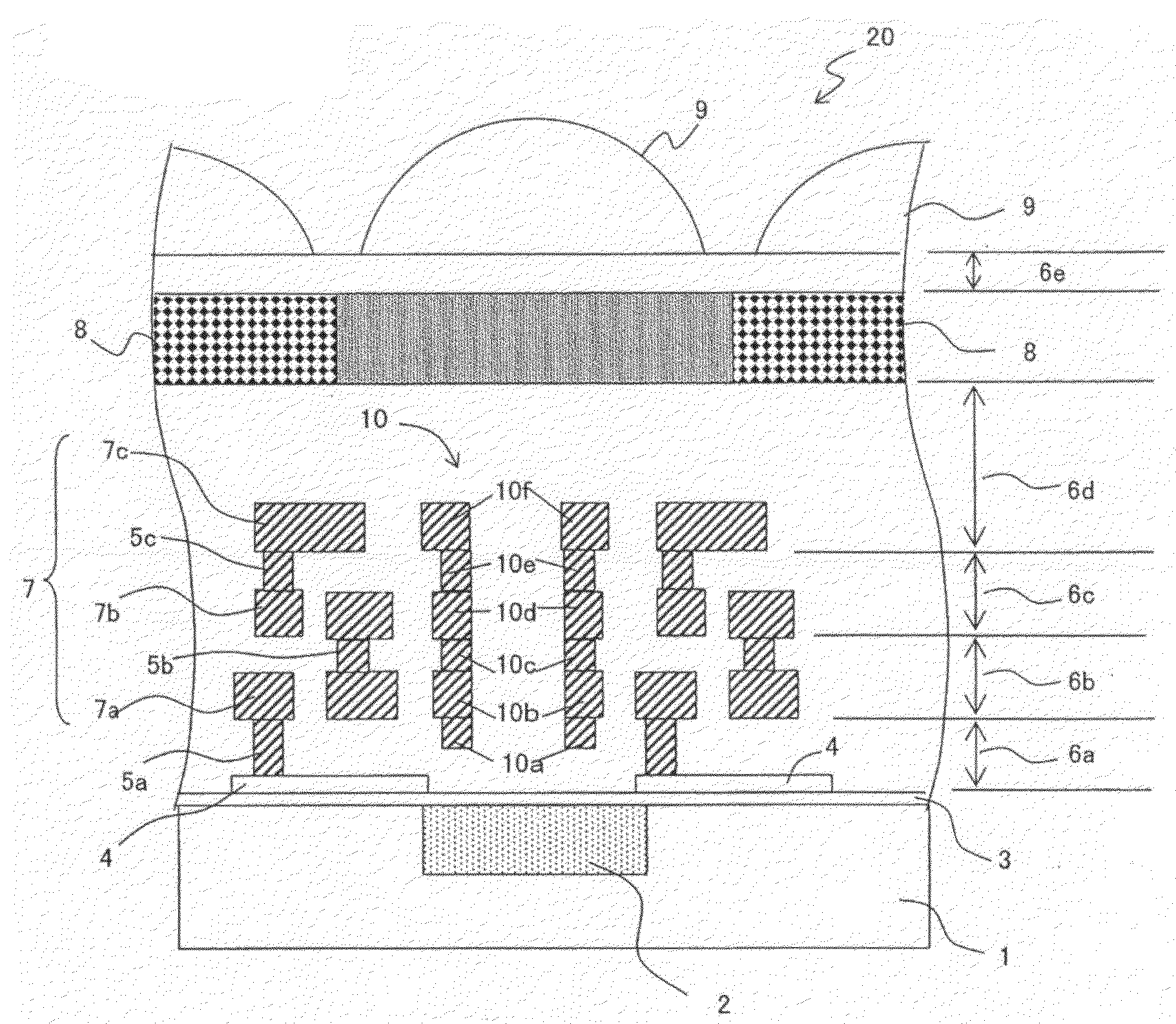
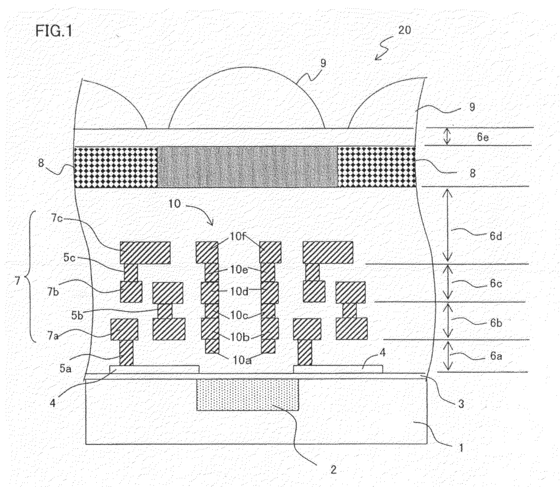
[0170]FIG. 1 is a longitudinal cross-sectional view showing an exemplary essential structure of a solid-state image capturing device 20 according to Embodiment 1.

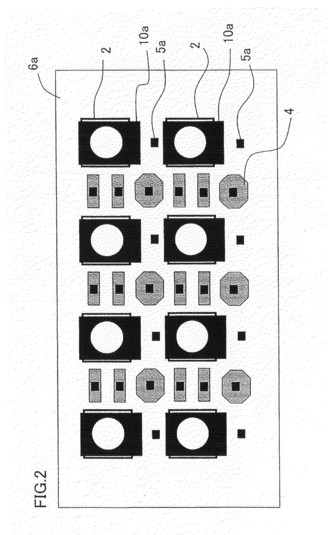
[0171]In FIG. 1, for the solid-state image capturing device 20 of Embodiment 1, a plurality of light receiving sections 2 such as photodiodes and the like are formed in two dimensions in a surface layer (image capturing region) of a semiconductor substrate 1, wherein the plurality of light receiving sections 2 function as photoelectric conversion sections for converting light of subject into a signal charge. Additionally, gate electrode films 4 as a lead electrode is formed via a gate insulation film 3 on this semiconductor substrate 1, and over this substrate, a plurality of contact plugs 5 (a first contact plug 5a, second contact plug 5b and third contact plug 5c) and / or a plurality of interlayer insulation films 6 (a first insulation film 6a, second insulation film 6b, third insulation film 6c, and fourth insulation film...

embodiment 2

[0195]Embodiment 1 has described the case where an optical waveguide 10 is formed by sequentially laminating a plurality of tubular optical waveguide tube portions 10a to 10f with one layer vertically at one time as the contact plugs 5 or wiring layers 7 being formed.

[0196]Embodiment 2 describes a case where two layers of the optical waveguide tube portions 10a to 10f are simultaneously laminated at one time (with lower layers being smaller size-wise and upper layers larger), yet depending on the alignment accuracy of the optical waveguide tube portions 10a to 10f, to reduce unevenness of the alignment of the metal surfaces resulting from vertically laminating the optical waveguide tube portions 10a to 10f.

[0197]FIG. 8 is a longitudinal cross-sectional view showing an exemplary essential structure of a solid-state image capturing device 20A according to Embodiment 2 of the present invention. Members attaining similar effects as those shown in FIG. 1 are denoted with the same refere...

embodiment 3

[0212]Embodiment 1 has described the case where an optical waveguide 10 is formed by sequentially laminating a plurality of tubular optical waveguide tube portions 10a to 10f with one layer vertically at one time as the contact plugs 5 or wiring layers 7 being formed, and Embodiment 2 has described the case where two layers of the optical waveguide tube portions 10a to 10f are simultaneously laminated at one time to reduce unevenness of the alignment of the metal surfaces resulting from vertically laminating the optical waveguide tube portions 10a to 10f. Embodiment 3 describes a case where three or five of the lower layers of the optical waveguide tube portions 10a to 10f are laminated at one time to reduce unevenness of the alignment of the metal surfaces resulting from vertically laminating the optical waveguide tube portions 10a to 10f.

[0213]FIG. 9 is a longitudinal cross-sectional view showing an exemplary essential structure of a solid-state image capturing device 20B accordi...


PUM


Abstract

A solid-state image capturing device according to the present invention is provided, in which a plurality of conductive films is formed via respective insulation films, and an optical waveguide is formed above a light receiving section, a plurality of light receiving sections is provided in a surface portion of a semiconductor substrate, and the plurality of conductive films is formed on a region other than a region right above the light receiving section, wherein a plural-layered optical waveguide tube is formed as the optical waveguide, with the same material as at least one of the plural-layered conductive films.

Description

[0001]This Nonprovisional Application claims priority under 35 U.S.C. §119(a) on Patent Application 2007-074998 filed in Japan on Mar. 22, 2007, the entire contents of which are hereby incorporated by reference.BACKGROUND OF THE INVENTION[0002]1. Field of the Invention[0003]The present invention relates to: a solid-state image capturing device (e.g., CMOS image sensor, CCD image sensor and the like) where an optical waveguide region is formed on each of the plurality of light receiving sections formed on a semiconductor substrate; a method for manufacturing the solid-state image capturing device; and an electronic information device using the solid-state image capturing apparatus as an image capturing section.[0004]2. Description of the Related Art[0005]A conventional solid-state image capturing device is known to have a structure in which an interlayer insulation film is processed on each of the light receiving sections that are a plurality of photoelectric conversion sections for ...

Claims


Application Information

Patent Timeline
IPC IPC(8): H01L31/0232H01L31/18H01L27/14H04N5/335H04N5/357H04N5/369H04N5/374
CPCH01L27/14603H01L27/14621H01L27/14623H01L27/14625H01L27/14627H01L27/14632H01L27/14636H01L27/14645H01L27/14685H01L27/14687H01L27/146
Inventor ISHIBE, SHOUICHI
Owner SHARP KK
Why Eureka
Try Eureka