Delay Circuit and Video Signal Processing Circuit Using the Same

Inactive Publication Date: 2008-10-16
SEMICON COMPONENTS IND LLC
View PDF3 Cites 7 Cited by
  • Summary
  • Abstract
  • Description
  • Claims
  • Application Information

AI Technical Summary

Benefits of technology

[0019]In order to solve the above problems, according to a main aspect of the present invention there is provided a delay circuit acquiring an output signal delayed from an input signal, comprising: a switched capacitor group that includes a plurality of switched capacitor units, wherein each of the plurality of switched capacitor units has a switching element, and a capacitive element which is charged / discharged by turning on / off the switching element, and wherein the plurality of switched capacitor units are connected such that the input signal is input in common to all of the plurality of switched capacitor units and such that the capacitive elements are charged as well as such that the capacitive elements are discharged to allow the output signal to be output from each of the plurality of switched capacitor units; and a switching control unit that performs on / off control of each of the switching elements of the plurality of switched capacitor units, to cause each of the capacitive elements of the plurality of switched capacitor units to be charged in sequence based on the input signal, and that, upon causing the each of the capacitive elements to be charged in sequence based on the input signal, causes the capacitive element charged last time to be discharged, to allow the output signal to be output in sequence from each of the plurality of switched capacitor units, and that, upon on / off switching of each of the switching elements of the plurality of switched capacitor units, performs control of all of the switching elements of the plurality of switched capacitor units so as to be turned off.

Problems solved by technology

Accordingly, the following problems may occur in the case of using the switched capacitor circuit as the delay circuit.

Method used


Image

  • Delay Circuit and Video Signal Processing Circuit Using the Same
  • Delay Circuit and Video Signal Processing Circuit Using the Same
  • Delay Circuit and Video Signal Processing Circuit Using the Same

Examples


Embodiment Construction

. OF THE INVENTION

[0036]At least the following details will become apparent from the descriptions of this specification and of the accompanying drawings.

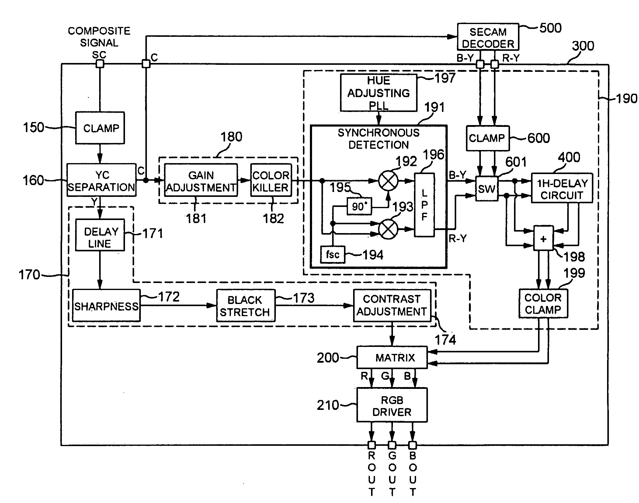
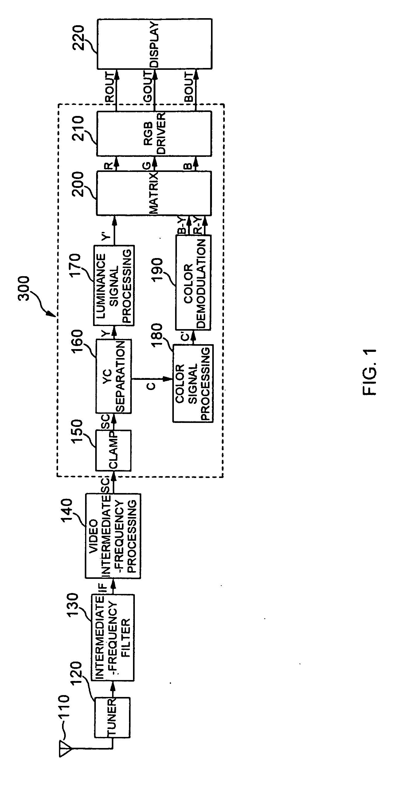
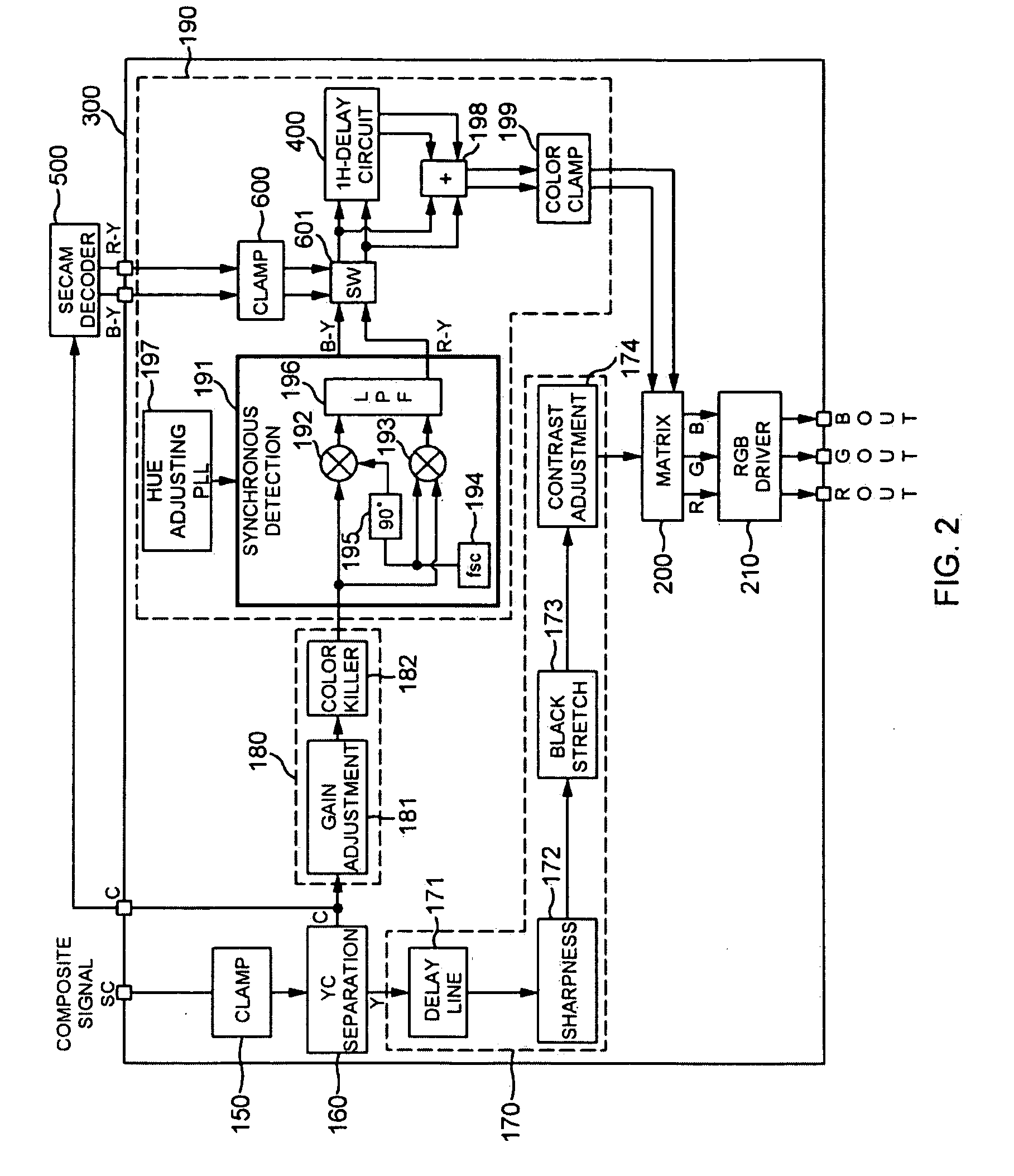
[0037]FIG. 1 is a configuration diagram of a television receiving system according to the present invention. A tuner 120 is a front-end processing circuit that extracts signals of a channel to be received among video signals of television broadcasting which are received at an antenna 110, and that thereafter amplifies and outputs the extracted signals. Note that the video signals of television broadcasting conform to the PAL system or the SECAM system and have three-primary-color (R, G, B) information on colors captured as an image by a television camera.

[0038]An intermediate-frequency filter 130 is a filter that extracts only intermediate-frequency signals IF from signals output from the tuner 120.

[0039]A video intermediate-frequency processing circuit 140 is a circuit that detects the intermediate-frequency signals IF extracted by...


PUM


Abstract

A delay circuit is disclosed. A switched-capacitor group includes a plurality of switched-capacitor units, each of which have a switching element and a capacitive element charged/discharged by turning on/off the switching element. The switched-capacitor units are connected such that the input signal is input in common to all of the switched-capacitor units and the capacitive elements are charged as well such that the capacitive elements are discharged to allow the output signal to be output from the switched-capacitor units. A switching control unit performs on/off control of the switching elements to cause the capacitive elements to be charged in sequence based on the input signal, causing the capacitive element charged last time to be discharged to allow the output signal to be output in sequence from the switched-capacitor units, and performs control of all of the switching elements to be turned off upon on/off switching of the switching elements.

Description

CROSS-REFERENCE TO RELATED APPLICATION[0001]This application claims the benefit of priority to Japanese Patent Application No. 2005-286082, filed Sep. 30, 2005, of which full contents are incorporated herein by reference.BACKGROUND OF THE INVENTION[0002]1. Field of the Invention[0003]The present invention relates to a delay circuit and a video signal processing circuit using the delay circuit.[0004]2. Description of the Related Art[0005]Analog color television systems which are employed in the world are broadly divided into three systems, i.e., NTSC (National Television Standards Committee) system employed mainly in Japan and North / Central America, PAL (Phase Alternation by Line) system employed mainly in the West European countries, and SECAM (SEquential Couleur A Memoire) system employed mainly in the East European countries. The NTSC system is a system of an interlaced scanning of 30 frames / sec, each frame having 525 horizontal scanning lines, with a horizontal scanning frequency...

Claims


Application Information

Patent Timeline
Patent Type & Authority Applications(United States)
IPC IPC(8): H04N9/77H03H11/26H03H19/00H04N9/64
CPCH03H11/265H04N9/66H04N9/78H01L21/18H01L29/762H04N9/77
Inventor SERIZAWA, SHUNSUKE
Owner SEMICON COMPONENTS IND LLC
Why Eureka
Try Eureka