Packaging substrate and method for manufacturing the same

a packaging substrate and substrate technology, applied in the direction of conductive pattern formation, semiconductor/solid-state device details, fixed connections, etc., can solve the problems of reduced joint strength, shortening the service life of packaging substrates, and reducing the strength of joints, so as to improve the service life and reduce the cost of packaging substrates. the effect of reducing the number of joints

Inactive Publication Date: 2008-10-23
PHOENIX PRECISION TECH CORP
View PDF2 Cites 27 Cited by
  • Summary
  • Abstract
  • Description
  • Claims
  • Application Information

AI Technical Summary

Benefits of technology

[0009]In view of the above-mentioned disadvantages, the object of the present invention is to provide a packaging substrate to increase the joint surface area between metal bumps and conductive pads and further inhibit the joint crack generally occurring in a conventional packaging substrate. Accordingly, the reliability of the packaging substrate can be enhanced, and the packaging substrate can be employed for meeting the trend of reducing the critical dimension of circuits of the substrate.

Problems solved by technology

Thereby, the reduced joint strength cannot always bear the stress between the chip and the substrate, and the matter of joint crack becomes serious.
Although the aforementioned structure can be used to electrically connect with a chip, it falls short of demand for package structure with high-density integration and miniaturization, owing to the trend of reducing the critical dimension (such as minimum line width), such that the reduced joint surface area between the metal bumps 14 and the conductive pads 12 makes the joint strength fail to bear the stress between the chip and the substrate, thereby the matter of joint crack frequently occurs and the reliability requirement of the product cannot be met.

Method used


Image

  • Packaging substrate and method for manufacturing the same
  • Packaging substrate and method for manufacturing the same
  • Packaging substrate and method for manufacturing the same

Examples


embodiment

Structure Embodiment

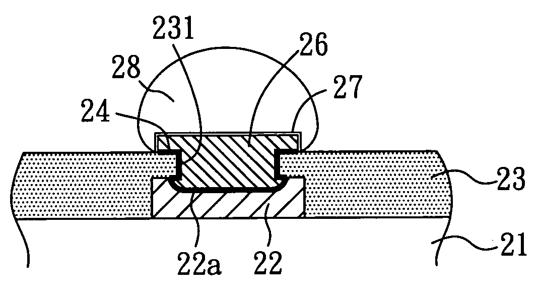
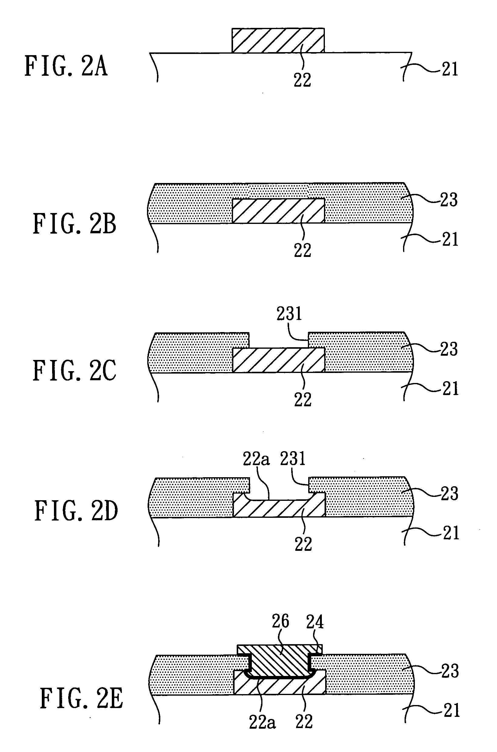
[0025]As shown in FIG. 2G, the packaging substrate of the present embodiment comprises: a substrate body 21, having a plurality of conductive pads 22 on the surface thereof, wherein the top surfaces of the conductive pads 22 have a concave 22a each; a solder mask 23, disposed on the surface of the substrate body 21 and having a plurality of openings 231 to correspondingly expose the concaves 22a of the conductive pads 22; and a plurality of metal bumps 26, disposed correspondingly in the openings 231 of the solder mask 23 and over the concaves 22a of the conductive pads 22. Herein, the metal bumps 26 are higher than the surface of the solder mask 23, and the parts of metal bumps 26 higher than the surface of the solder mask 23 have a width bigger than the size of the openings 231 of the solder mask 23. Also, the parts of metal bumps 26 higher than the surface of the solder mask 23 can have a width equal to the size of the openings 231 of the solder mask 23 (not s...


PUM

PropertyMeasurementUnit
conductiveaaaaaaaaaa
widthaaaaaaaaaa
sizeaaaaaaaaaa

Abstract

The present invention relates to a packaging substrate and a method for manufacturing the same. The packaging substrate includes: a substrate body, having a plurality of conductive pads on the surface thereof, wherein the top surfaces of the conductive pads have a concave each; a solder mask, disposed on the surface of the substrate body and having a plurality of openings to correspondingly expose the concaves of the conductive pads each; and a plurality of metal bumps, disposed correspondingly in the openings of the solder mask and over the concaves of the conductive pads. The present invention increases the joint surface area between the metal bumps and the conductive pads so as to inhibit the joint crack and improve the reliability of the conductive structure of the packaging substrate.

Description

BACKGROUND OF THE INVENTION[0001]1. Field of the Invention[0002]The present invention relates to a packaging substrate and a method for manufacturing the same and, more particularly, to a packaging substrate that can increase the joint surface area between conductive pads and metal bumps and a method for manufacturing the same.[0003]2. Description of Related Art[0004]As the electronic industry develops rapidly, research accordingly moves towards electronic devices with multifunction and high efficiency. Hence, circuit boards with many active and passive components and circuit connections have advanced from being single-layered boards to multiple-layered boards so that the packaging requirements such as integration and miniaturization in semiconductor packaging can be met. Furthermore, interlayer connection technique is also applied in this field to expand circuit layout space in a limited circuit board and to meet the demand of the application of high-density integrated circuits.[00...

Claims


Application Information

Patent Timeline
Patent Type & Authority Applications(United States)
IPC IPC(8): H01R12/04H05K3/10
CPCH01L23/49816H01R12/57H05K3/06H05K3/243H05K3/28Y10T29/49155H05K2201/0367H05K2201/09436H05K2201/09745H05K2203/0353H01L24/11H05K3/4007H01L2224/05001H01L2224/05022H01L2224/05111H01L2224/05147H01L2224/05155H01L2224/05166H01L2224/05171H01L2224/05572H01L2224/05611H01L2224/05639H01L2224/05644H01L2224/05655H01L2224/05671H01L2924/00014H01L2924/14H01L2924/00H01L2924/01024H01L2924/01082H01L2924/01022H01L2924/01079H01L2924/01046
Inventor HU, WEN-HUNG
Owner PHOENIX PRECISION TECH CORP
Why Eureka
Try Eureka