Liquiid crystal on silicon (LCOS) display and package thereof

a liquid crystal display and liquid crystal technology, applied in the field of liquid crystal display (lcd), can solve the problems of high cost and complex manufacturing process, and achieve the effects of improving package yield, increasing area efficiency and system integration, and reducing manufacturing cos

Inactive Publication Date: 2008-10-30
HIMAX TECH LTD
View PDF7 Cites 24 Cited by
  • Summary
  • Abstract
  • Description
  • Claims
  • Application Information

AI Technical Summary

Benefits of technology

[0013]Accordingly, the present invention is directed to a LCOS display. The display utilizes the spare die area to incorporate more functions for increasing area efficiency and system integration, improving package yield, and decreasing manufacturing cost.

Problems solved by technology

The conventional LCOS display has a lot of components such that that the manufacturing process is complex and the cost is high.

Method used


Image

  • Liquiid crystal on silicon (LCOS) display and package thereof
  • Liquiid crystal on silicon (LCOS) display and package thereof
  • Liquiid crystal on silicon (LCOS) display and package thereof

Examples


Embodiment Construction

[0025]Reference will now be made in detail to the present preferred embodiment of the invention, examples of which are illustrated in the accompanying drawings. Wherever possible, the same reference numbers are used in the drawings and the description to refer to the same or like parts.

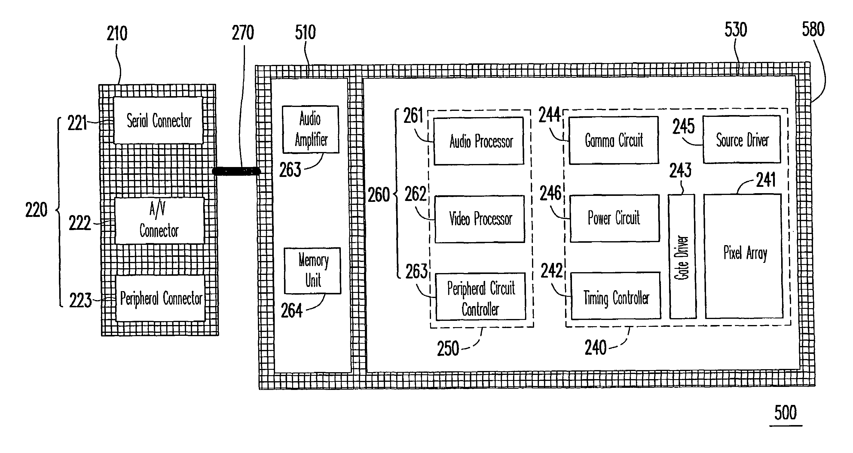
[0026]FIG. 2A is a block diagram of the LCOS display 200. The display 200 comprises a PCB 210, an interface module 220, a first silicon chip 230, and a flat cable 270. The interface module 220 is disposed on the PCB 210 and is used to receive an A / V signal. The first silicon chip 230 comprises a display area 240, a processing area 250 and a metal layer 310 (shown in FIG. 2B). The display area 240 comprises a pixel array 241 formed on the first silicon chip 230. The processing area 250 comprises a processing unit 260 formed on the first silicon chip 230. The metal layer 310 is formed on the first silicon chip 230 for electrically connecting the display area 240 with the processing area 250. The flat ca...


PUM

PropertyMeasurementUnit
areaaaaaaaaaaa
processing areaaaaaaaaaaa
conductiveaaaaaaaaaa

Abstract

The present invention provides a LCOS display. The display comprises a first PCB, an interface module, a first silicon chip, and a flat cable. The interface module is disposed on the first PCB and used to receive an audio and video signal. The first silicon chip comprises a display area, a processing area, and a metal layer. The display area comprises a pixel array in a LCOS panel formed on the first silicon chip. The processing area comprises a processing unit formed on the first silicon chip. The metal layer is formed on the first silicon chip for electrically connecting the display area with the processing area. The flat cable is used to electrically connect the interface module with the processing unit.

Description

CROSS-REFERENCE TO RELATED APPLICATION[0001]This application claims the priority benefit of U.S.A. provisional application Ser. No. 60 / 914,043, filed on Apr. 26, 2007. The entirety of the above-mentioned patent application is hereby incorporated by reference herein and made a part of this specification.BACKGROUND OF THE INVENTION[0002]1. Field of Invention[0003]The present invention generally relates to a liquid crystal display (LCD), and more particularly to a liquid crystal on silicon (LCOS) display and package thereof.[0004]2. Description of Prior Art[0005]FIG. 1A is a block diagram of an LCOS display 100. The LCOS display 100 comprises a LCOS panel 103, an audio and video (A / V) system board 102, and an input and output (I / O) connector board 101. The I / O connector board 101 is electrically connected to the A / V system board 102 via a signal cable 104, and the A / V system board 102 is electrically connected to the LCOS panel 103 via a FPC cable 105. The I / O connector board 101 is us...

Claims


Application Information

Patent Timeline
Patent Type & Authority Applications(United States)
IPC IPC(8): G02F1/133G09G3/36
CPCG09G3/2092G09G2300/0408G02F1/133G02F1/1345
Inventor CHEN, KUEI-HSIANGBU, LIN-KAI
Owner HIMAX TECH LTD
Why Eureka
Try Eureka