Stacking fault reduction in epitaxially grown silicon

a technology of epitaxial growth and stacking faults, applied in semiconductor/solid-state device manufacturing, basic electric elements, electric devices, etc., can solve the problems of reducing the structure of growing stacking faults, reducing stacking faults, and often occurring stacking faults, etc., to reduce stacking faults and suppress stacking faults

Inactive Publication Date: 2008-10-30
GLOBALFOUNDRIES INC
View PDF9 Cites 2 Cited by
  • Summary
  • Abstract
  • Description
  • Claims
  • Application Information

AI Technical Summary

Benefits of technology

[0010]Methods and a structure are disclosed to suppress stacking faults in epitaxially grown silicon for use in hybrid surface orientation structures. In one embodiment, a method includes depositing a silicon nitride liner over a silicon oxide liner in an opening, etching to remove the silicon oxide liner and silicon nitride liner on a lower surface of the opening, undercutting the silicon nitride liner adjacent to the lower surface, and epitaxially growing silicon in the opening. The silicon has reduced stacking faults because of the negative slope created by the undercut.

Problems solved by technology

Fabricating the above-described hybrid orientation logic devices presents challenges.
One challenge relative to the above-described technique, however, is growing stacking fault reduced structure.
Stacking faults are planer defects which often occur in epitaxial films when the crystal stacking sequence is disrupted because of local environmental changes during growth, e.g., impurities or surface imperfections.
The defects are characterized by the fact that the displacement between planes on either side of the defect is not a perfect crystal translation vector for the material in question.

Method used


Image

  • Stacking fault reduction in epitaxially grown silicon
  • Stacking fault reduction in epitaxially grown silicon
  • Stacking fault reduction in epitaxially grown silicon

Examples


Embodiment Construction

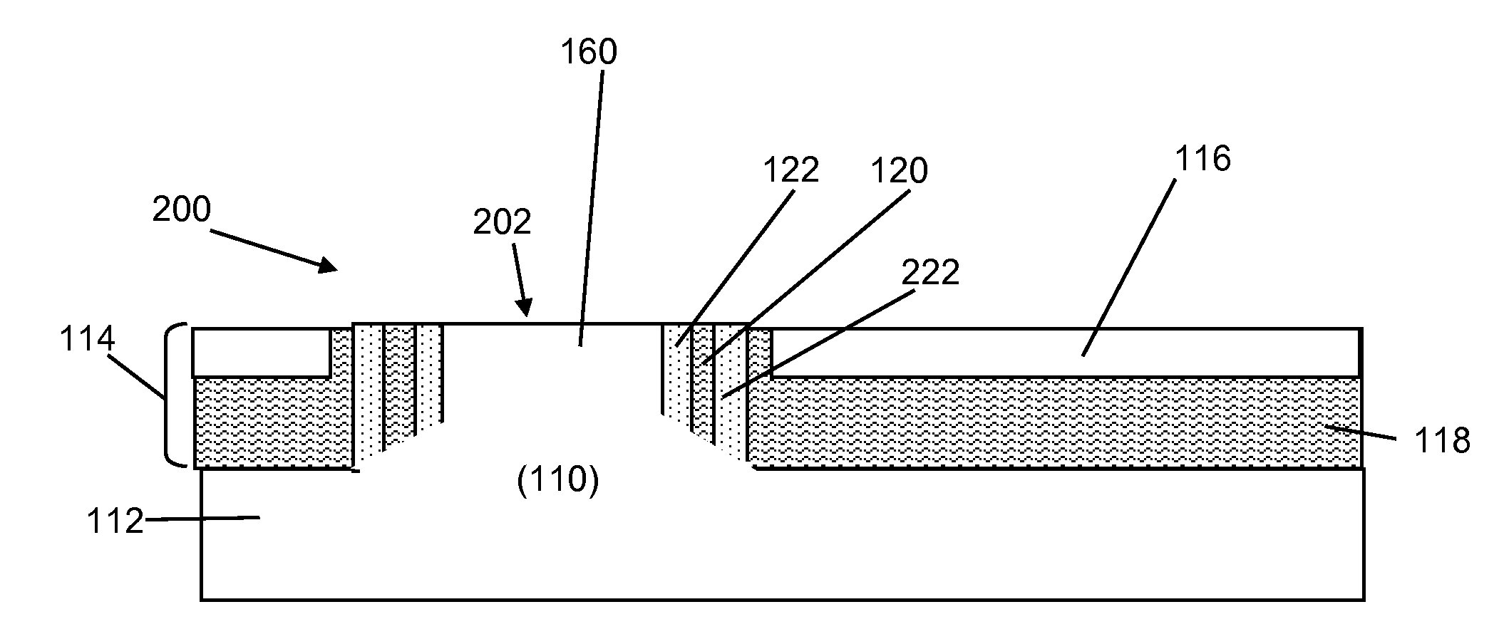
[0021]Turning to FIGS. 2-8, various embodiments of a method of epitaxially growing stacking fault reduced silicon 160 (FIGS. 7-8) in an opening 130 (FIGS. 4-5) to silicon will be described. The method is advantageous as part of a method forming an intermediate stacking fault reduced hybrid surface orientation structure 200 (FIG. 7).

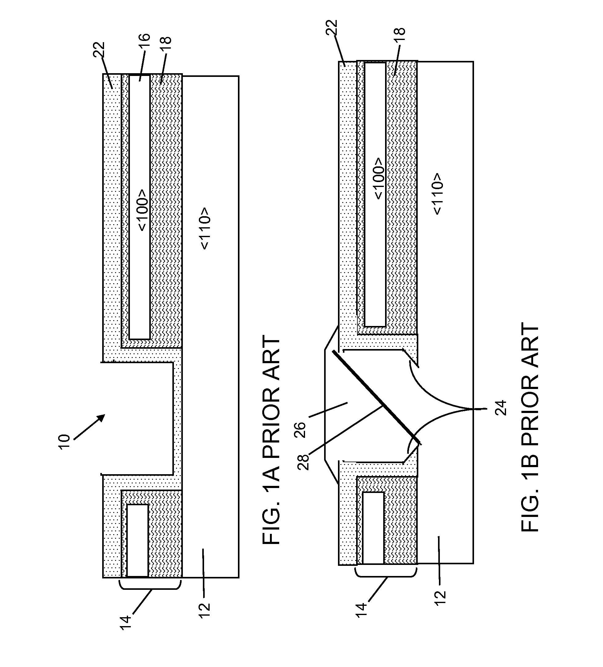
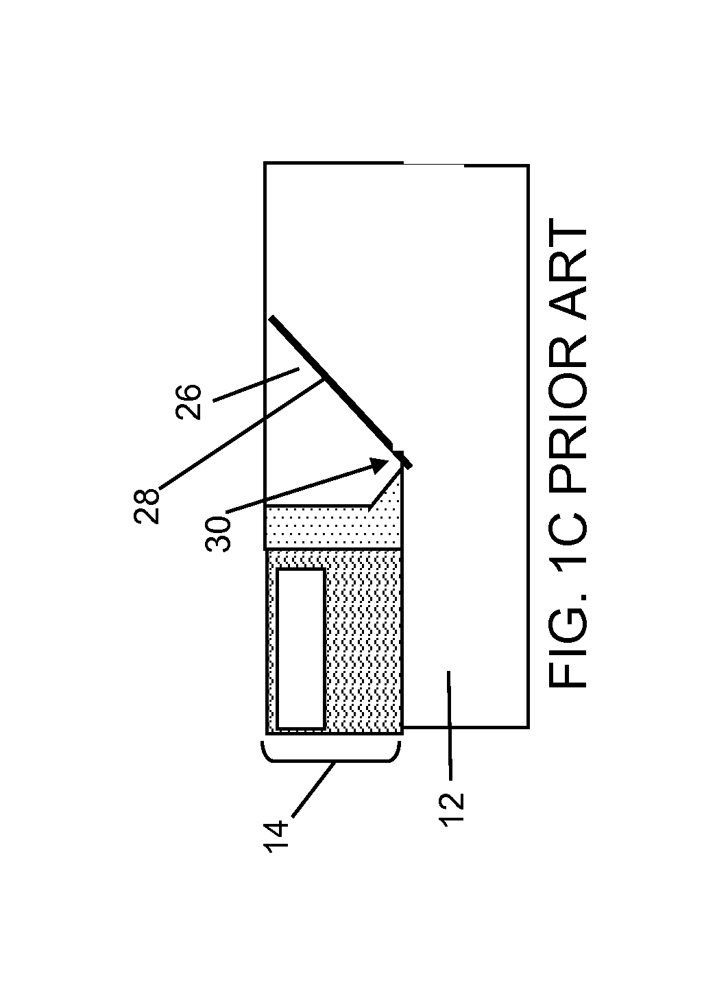
[0022]Turning to FIG. 2, if the method is used to form stacking fault reduced surface orientation structure 200 (FIG. 7), first, a silicon-on-insulator (SOI) substrate 114 is provided adhered to a bulk silicon substrate 112. SOI substrate 114 includes a silicon 116 within a buried silicon oxide (BOX) layer 118. As understood, silicon 116 of SOI substrate 114 has a different surface orientation than that of bulk silicon substrate 112. For example, as shown, silicon 116 has a surface orientation of (100), while bulk silicon substrate 112 has a surface orientation of (110). The surface orientations illustrated are only examples, and any different surface ori...


PUM

PropertyMeasurementUnit
stacking faultaaaaaaaaaa
thicknessaaaaaaaaaa
orientation structureaaaaaaaaaa

Abstract

Methods are disclosed for providing stacking fault reduced epitaxially grown silicon for use in hybrid surface orientation structures. In one embodiment, a method includes depositing a silicon nitride liner over a silicon oxide liner in an opening, etching to remove the silicon oxide liner and silicon nitride liner on a lower surface of the opening, undercutting the silicon nitride liner adjacent to the lower surface, and epitaxially growing silicon in the opening. The silicon is substantially reduced of stacking faults because of the negative slope created by the undercut.

Description

[0001]This patent application is a divisional of U.S. patent application Ser. No. 11 / 456,326, filed Jul. 10, 2006, currently pending.BACKGROUND OF THE INVENTION[0002]1. Technical Field[0003]The invention relates generally to microelectronics fabrication, and more particularly, to methods and structure with reduced stacking faults in epitaxially grown silicon.[0004]2. Background Art[0005]Performance improvement of semiconductor devices is a never-ending endeavor for manufacturers of those devices. One challenge currently faced by the semiconductor industry is implementing memory and logic devices on a single chip while maintaining process simplicity and transistor performance. These devices are referred to as “system-on-chips” (SoC) because the electronics for a complete, working product are contained on a single chip. One approach that is currently employed to improve performance of a SoC is to fabricate the different types of logic devices on silicon substrates having optimal surfa...

Claims


Application Information

Patent Timeline
Patent Type & Authority Applications(United States)
IPC IPC(8): H01L21/76
CPCH01L21/02381H01L21/02433H01L21/02532H01L21/02609H01L21/02639H01L21/84
Inventor WANG, YUN-YUBLACK, LINDAHOLT, JUDSON R.LEE, WOO-HYEONGLUNING, SCOTTSHERAW, CHRISTOPHER D.
Owner GLOBALFOUNDRIES INC
Why Eureka
Try Eureka