Silicon carbide with high thermal conductivity

a silicon carbide and thermal conductivity technology, applied in the direction of polycrystalline material growth, condensed vapor, chemically reactive gases, etc., can solve the problems of high heat generation of many electronic devices, material failure, and insufficient heat dissipation speed of electronic devices, so as to reduce stacking faults

Inactive Publication Date: 2008-10-21
TOKAI CARBON CO LTD
View PDF11 Cites 2 Cited by
  • Summary
  • Abstract
  • Description
  • Claims
  • Application Information

AI Technical Summary

Benefits of technology

[0013]The present invention is directed to a freestanding polycrystalline silicon carbide (SiC) produced by chemical vapor deposition (CVD). The SiC of the present invention has reduced stacking faults, and a thermal conductivity of at least 375 W / mK, a property that is advantageous in dissipating heat. The SiC can be employed in high heat load apparatus where semiconductors are manufactured without concern that the SiC may degenerate. The SiC also is employed in active thermoplastic coolers as well as heat sinks and fans in electronic devices where high heat is generated.
[0016]Advantageously, the SiC of the present invention has a high thermal conductivity such that the SiC can readily be employed as components of apparatus that make semiconductors where high heat loads are generated. Such heat loads may exceed 300 Kcal / min. Also, the SiC can be employed in active thermocoolers, heat sinks and fans in high heat generating electronic devices.
[0018]Another objective of the present invention is to provide a chemical vapor deposited, silicon carbide with reduced stacking faults.

Problems solved by technology

If materials that comprise the wafer and wafer holders have an insufficiently high thermal conductivity, the materials may fail, i.e., crack or fracture due to thermal stress.
During operation, many electronic devices generate high amounts of heat.
Without suitable thermoelectric coolers, heat sinks, or fans, the electronic devices can not dissipate heat fast enough and they degenerate or break down.
Thus such electronic devices would have short life spans, and would be inefficient for industries employing the devices.
However, single crystal SiC is difficult to produce in large enough sizes to employ in the manufacture of such materials as semiconductor furnace support components, and is considerably more expensive than polycrystalline SiC.
Unfortunately, polycrystalline SiC does not achieve the theoretical thermal conductivity of a single crystal of SiC due to the presence of grain boundaries, which scatter phonons or sound energy.
Accordingly, it is very difficult to predict a range, let alone a specific value, for the thermal conductivity of a chemical vapor deposited, polycrystalline SiC.
In addition, point, line and extended defects diminish the thermal conductivity of polycrystalline SiC.
Such defects add to the difficulty of preparing a SiC with a desired high thermal conductivity.
Another crystalline problem associated with polycrystalline SiC that may effect the thermal conductivity are stacking faults as suggested in W. Kowbel et al.
However, Kowbel et al. only achieved a maximum thermal conductivity of 140 W / mK.
Such low thermal conductivities are unsuitable for the demands of the semiconductor device and electronic device industries.
If such gaps in the crystalline lattice reduce the capacity of the SiC to conduct and dissipate heat, a “chiller”, such as a heat sink, composed of such material is not reliable in an electronic device where a high heat load is continuously generated.
Such high heat generation can readily damage electronic devices after about 200 hours of operation without an appropriate heat sink.
However, with the exceptions discussed below, few if any methods have been developed to provide a SiC with a thermal conductivity that exceeds 300 W / mK, let alone 375 W / mK.
Further, improved apparatus employed in manufacturing semiconductors are also generating very high quantities of heat, and require component parts having high thermal conductivities.
However, the methods described in the foregoing patents did not achieve a SiC with a thermal conductivity of greater than 300 W / mK.
For example, under conditions of high temperature and low MTS flow rates (which results in low MTS partial pressure), the grain size increases.
However, because of the crystalline defects in polycrystalline SiC discussed above, altering one or more of the aforementioned parameters does not provide a reliable means of obtaining a SiC having a specific thermal conductivity.

Method used


Image

  • Silicon carbide with high thermal conductivity
  • Silicon carbide with high thermal conductivity
  • Silicon carbide with high thermal conductivity

Examples


example 1

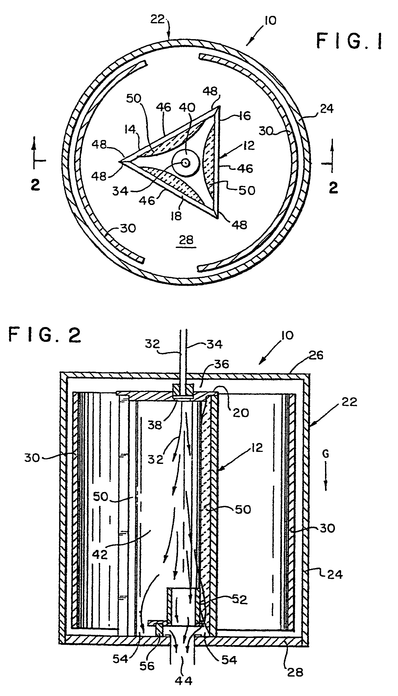
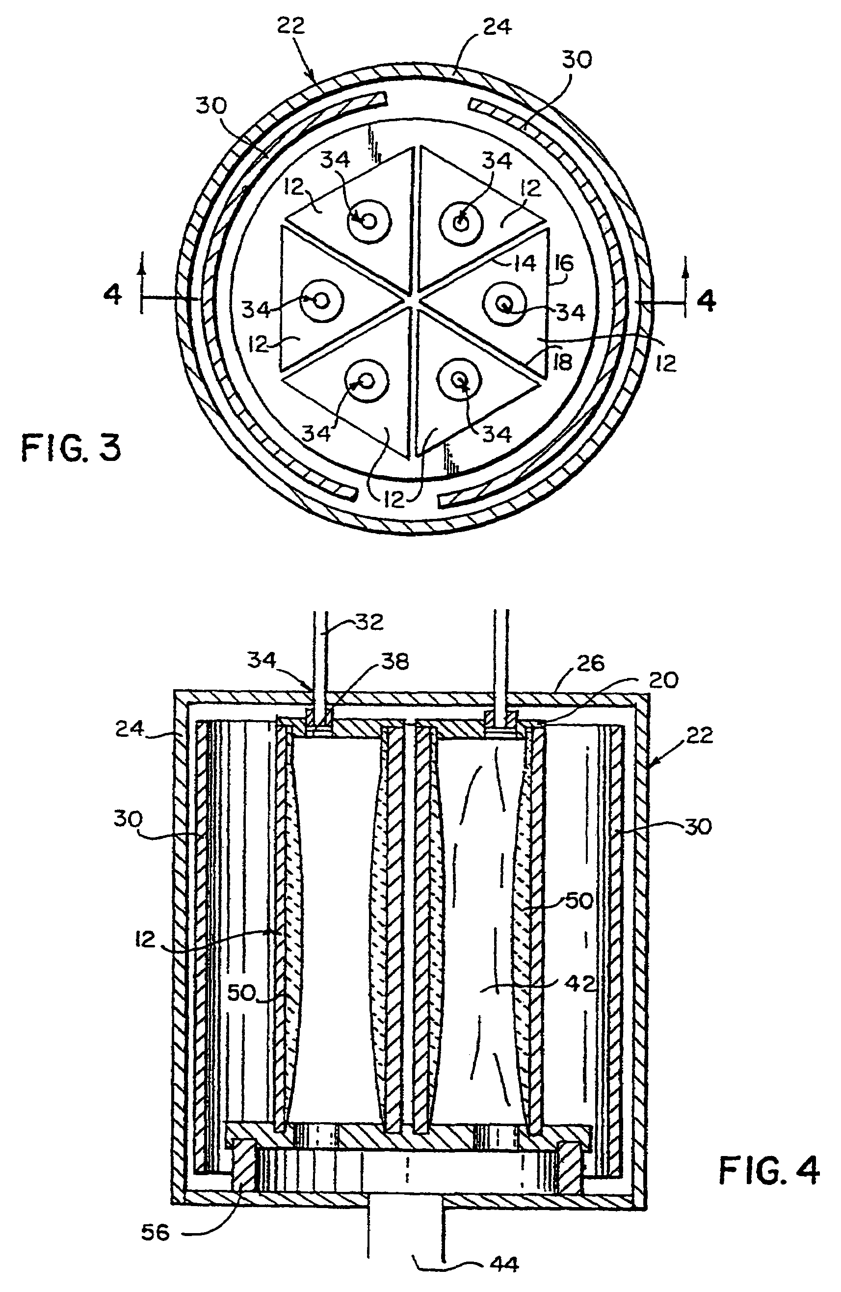
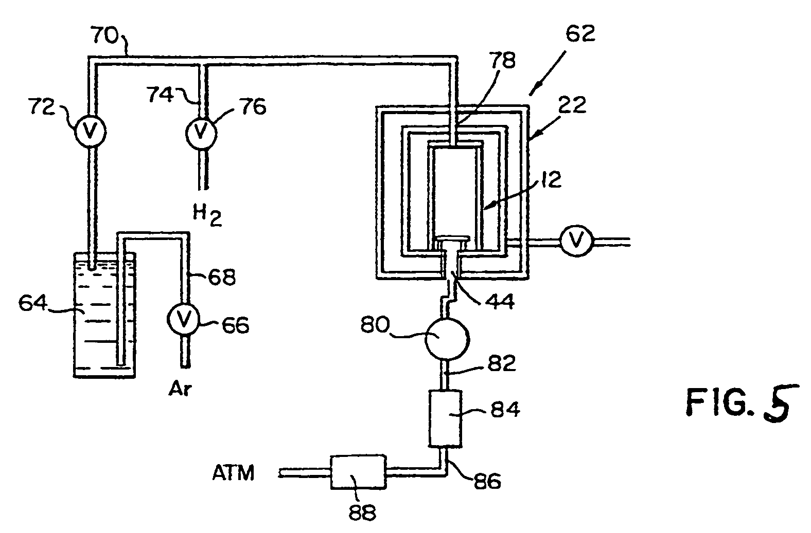
[0043]SiC was deposited in a triangular deposition setup consisting of six separate deposition boxes as shown in FIGS. 3 and 4. The size of each individual triangular deposition box used was optimized to produce high thermal conductivity SiC. The length of each box was about 78 inches and each side of the triangles was about 21 inches. The reagent flow was from top to bottom such that the reagent flow was parallel to the graphite mandrels. To produce CVD-deposited SiC in accordance with the invention, temperature, pressure, H2 / MTS ratio and deposition rate preferably is within the ranges set forth below, regardless of specific furnace design.

[0044]The temperature of the deposition chambers was about 1355° C. The furnace pressure was about 200 torr. The gas flow rate for H2 was about 67 slpm (standard liters per minute measured at atmosphere pressure and 20° C.), and the gas flow rate for MTS was about 11 slpm. Argon gas was employed as the carrier gas at a flow rate of about 69 slpm...


PUM

PropertyMeasurementUnit
grain sizeaaaaaaaaaa
temperatureaaaaaaaaaa

Abstract

A chemical vapor deposited, β phase polycrystalline silicon carbide having a high thermal conductivity and reduced stacking faults. The silicon carbide is synthesized under specific conditions using hydrogen gas and methyltrichlorosilane gas as reactants. The thermal conductivity of the silicon carbide is sufficiently high such that it can be employed as parts of apparatus and components of electrical devices where a high heat load is generated. Such components may include active thermoelectric coolers, heat sinks and fans.

Description

[0001]This application is a continuation of application(s) application Ser. No. 10 / 035,877 filed on Nov. 9, 2001 now U.S. Pat. No. 6,811,761. The nonprovisional application designated above, namely application Ser. No. 10 / 035,877, filed Nov. 9, 2001 claims the benefit of U.S. Provisional Application(s) No(s).: 60 / 247,267 FILING DATE Nov. 10, 2000BACKGROUND OF THE INVENTION[0002]The present invention is directed to an improved chemical vapor deposited (CVD) silicon carbide (SiC). More specifically, the present invention is directed to a chemical vapor deposited (CVD) silicon carbide (SiC) with reduced stacking faults and high thermal conductivity.[0003]Many manufacturing steps are involved in the production of semiconductor devices. Some steps in the manufacture of semiconductor devices involve rapid thermal processing where heat is necessarily applied and dissipated rapidly from the wafer and wafer holders in the processing of semiconductors. If materials that comprise the wafer and...

Claims


Application Information

Patent Timeline
Patent Type & Authority Patents(United States)
IPC IPC(8): C01B31/36C04B35/565C23C16/32C23C16/42
CPCC04B35/565C23C16/325
Inventor BRESE, NATHANIEL E.GOELA, JITENDRA S.PICKERING, MICHAEL A.
Owner TOKAI CARBON CO LTD
Why Eureka
Try Eureka