Wafer Bonding

a bonding and wafer technology, applied in the field of semiconductor/solid-state device manufacturing, electrical equipment, basic electric elements, etc., can solve the problems of reducing the wafer size, and reducing the bubbling effect of the wafer

Inactive Publication Date: 2008-10-30
TAIWAN SEMICON MFG CO LTD
View PDF16 Cites 49 Cited by
  • Summary
  • Abstract
  • Description
  • Claims
  • Application Information

AI Technical Summary

Problems solved by technology

During the thinning process, however, the wafer often cracks and chips because the edges of the wafer are unsupported.
These attempts, however, reduce the wafer size and often include additional timely processes.
Furthermore, these attempts may also require specialized equipment or may be incompatible with processes used by some fabricators.

Method used


Image

  • Wafer Bonding
  • Wafer Bonding
  • Wafer Bonding

Examples


Embodiment Construction

[0015]The making and using of the presently preferred embodiments are discussed in detail below. It should be appreciated, however, that the present invention provides many applicable inventive concepts that can be embodied in a wide variety of specific contexts. The specific embodiments discussed are merely illustrative of specific ways to make and use the invention, and do not limit the scope of the invention.

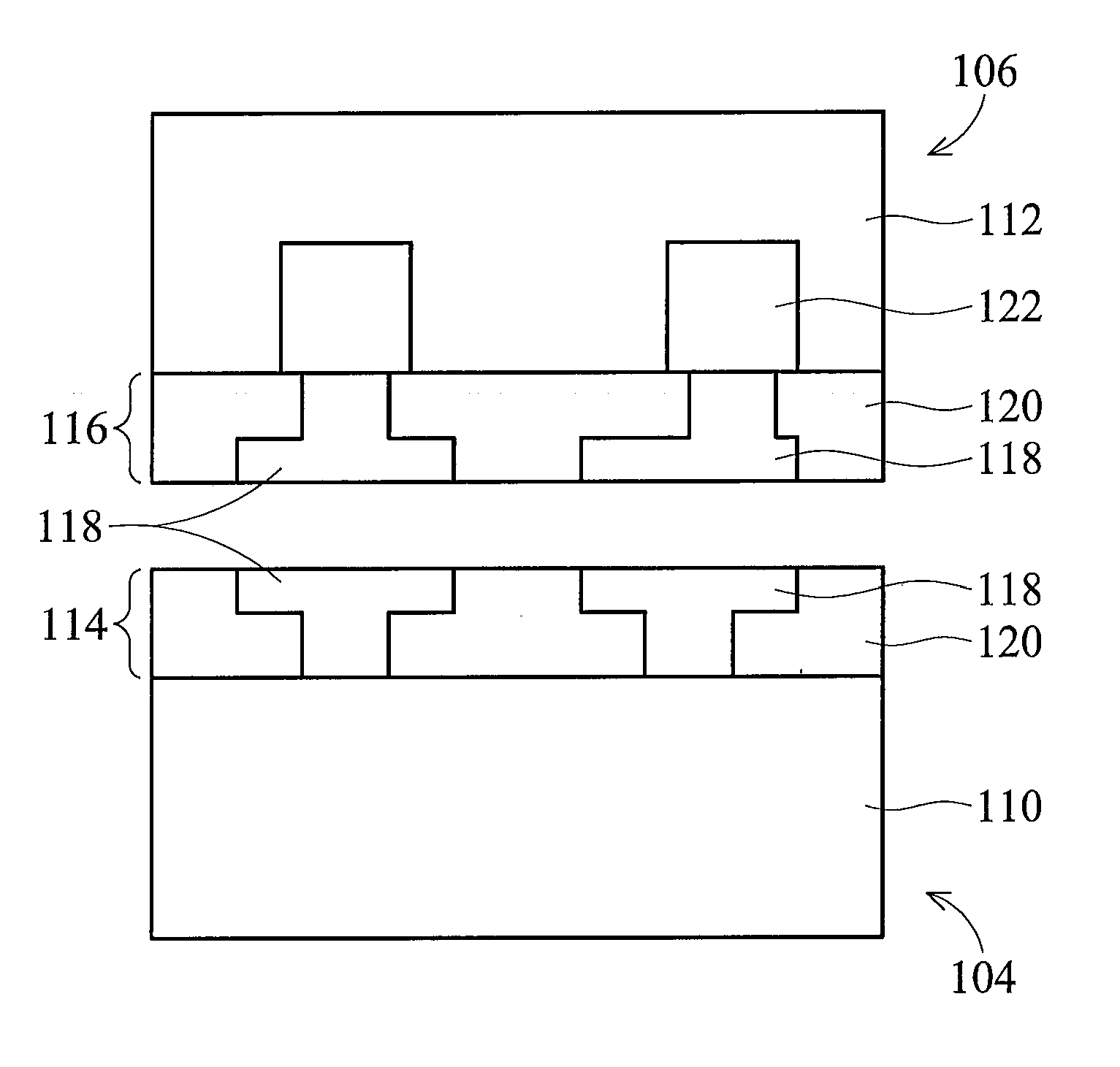
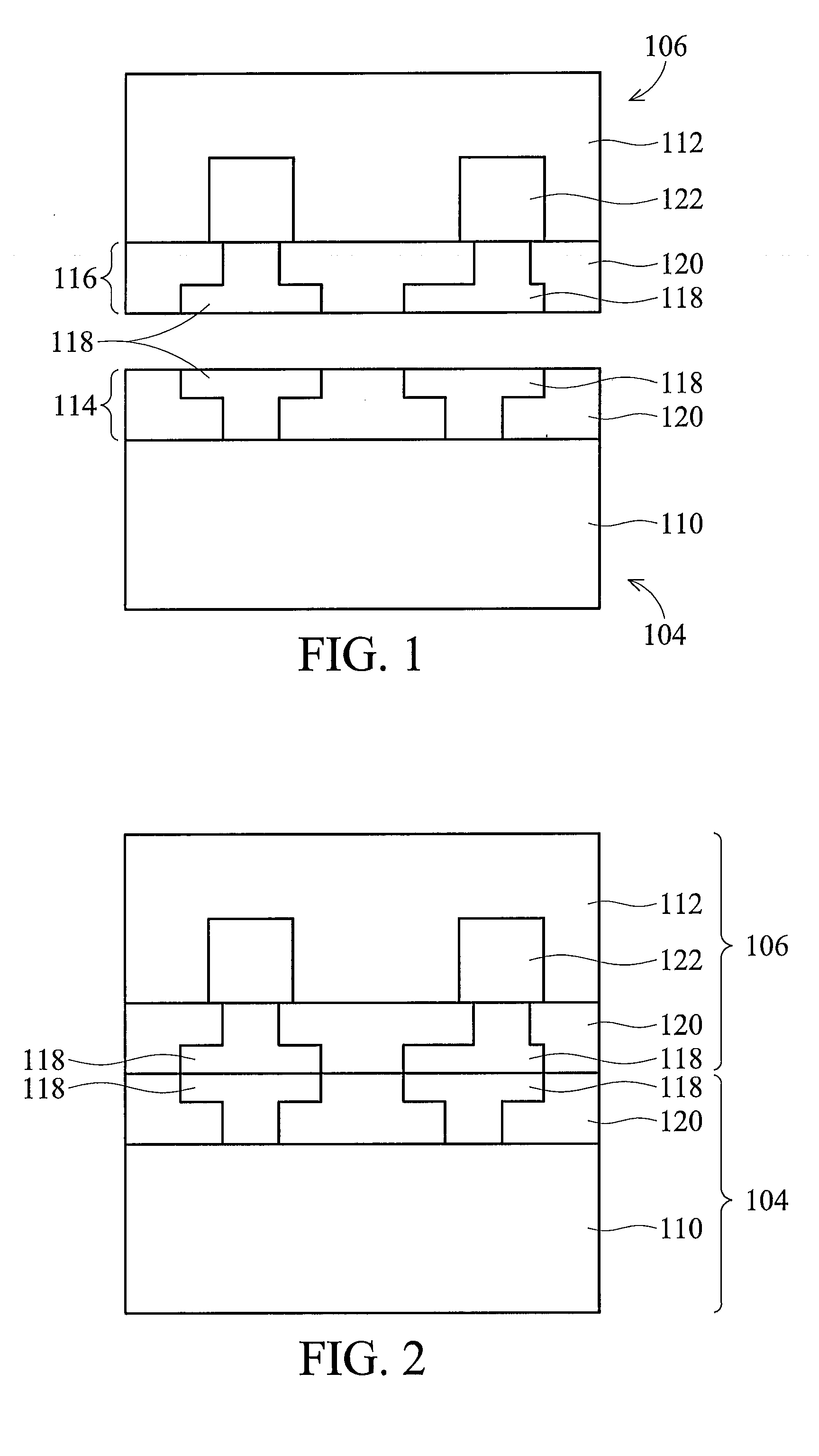
[0016]Referring first to FIG. 1, a first wafer 104 and a second wafer 106 are shown being prepared to be bonded in accordance with an embodiment of the present invention. The first wafer 104 and the second wafer 106 comprise a first semiconductor substrate 110 and a second semiconductor substrate 112, respectively, with electronic circuitry (not shown) formed thereon. The first semiconductor substrate 110 and the second semiconductor substrate 112 may each comprise bulk silicon, doped or undoped, or an active layer of a semiconductor-on-insulator (SOI) substrate. Generally, a...


PUM


Abstract

A method for providing a stacked wafer configuration is provided. The method includes bonding a first wafer to a second wafer. A filler material is applied in a gap formed along edges of the first wafer and the second wafer. The filler material provides support along the edges during a thinning and transportation process to help reduce cracking or chipping. The filler material may be cured to reduce any bubbling that may have occurred while applying the filler material. Thereafter, the second wafer may be thinned by grinding, plasma etching, wet etching, or the like. In some embodiments of the present invention, this process may be repeated multiple times to create a stacked wafer configuration having three or more stacked wafers.

Description

TECHNICAL FIELD[0001]The present invention relates generally to semiconductor structures, and more particularly, to bonding multiple wafers together to create a stacked wafer configuration.BACKGROUND[0002]Semiconductor chips used in electronic devices comprise a semiconductor die mounted on a carrier or a substrate. In an effort to increase the density and functionality of a semiconductor chip, attempts have been made to create 3D-ICs, or three-dimensional integrated circuits. Generally, 3D-ICs comprise a plurality of semiconductor dies stacked upon each other, such as one semiconductor die bonded on top of another semiconductor die. Electrical connections electrically couple contact pads on each of the stacked semiconductor dies to external contacts. The dies may include different functionality or simply increase the density of a single functionality, such as a memory.[0003]Generally, attempts at creating 3D-ICs have included bonding a first wafer on which a plurality of dies has b...

Claims


Application Information

Patent Timeline
Patent Type & Authority Applications(United States)
IPC IPC(8): H01L21/30
CPCH01L21/2007
Inventor YANG, KU-FENGWU, WENG-JINCHIOU, WEN-CHIHYU, CHEN-HUA
Owner TAIWAN SEMICON MFG CO LTD
Why Eureka
Try Eureka