Circuit and method for interconnecting stacked integrated circuit dies

a technology of integrated circuits and dies, which is applied in the field of integrated circuits, can solve the problems of affecting the operation of the circuit, the inability to route signals directly to the bonding pads on the lower die, and the overflow of the desired capacity of the memory device di

Active Publication Date: 2008-11-06
MICRON TECH INC
View PDF9 Cites 67 Cited by
  • Summary
  • Abstract
  • Description
  • Claims
  • Application Information

AI Technical Summary

Problems solved by technology

However, it is sometimes desirable to place two or more integrated circuit dies in a single package.
For example, if the integrated circuit is a memory device, such as a flash memory device, the desired capacity of the memory device may exceed the currently available capacity of memory device dies.
Signals generally cannot be routed directly to bonding pads on the lower die because the upper die covers the bonding pads on the lower die.
Yet economic considerations make this approach undesirable.
Also, this approach would not allow more than two dies to be stacked since the bonding pads on the middle die(s) would not be accessible.

Method used


Image

  • Circuit and method for interconnecting stacked integrated circuit dies
  • Circuit and method for interconnecting stacked integrated circuit dies
  • Circuit and method for interconnecting stacked integrated circuit dies

Examples


Embodiment Construction

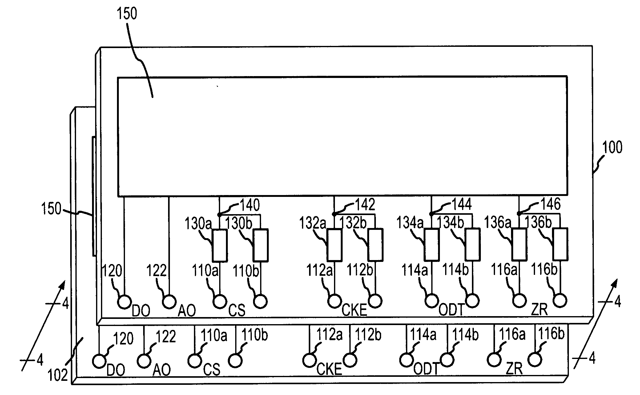
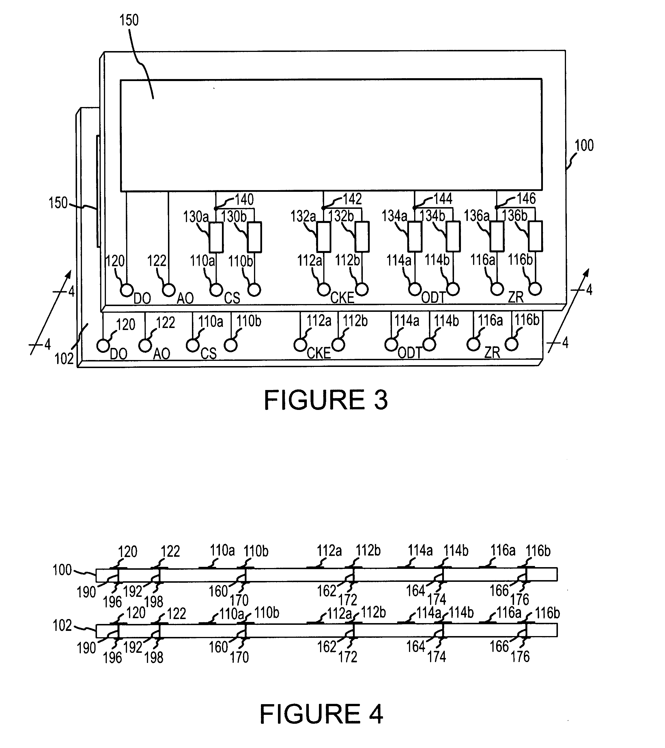
[0019]An improved technique for separately routing signals to and / or from stacked integrated circuit dies according to an embodiment of the invention is shown in FIG. 3. In the interests of brevity and clarity, FIG. 3 shows only two stacked integrated circuit dies 100, 102, it being understood that additional dies may be stacked on one another. The dies 100, 102 are identical to each other. Also, FIG. 3 shows only one data signal D0 and one address signal A0 that are common to both dies 100, 102, coupled to and / or from the dies 100, 102. However, it will be understood that a substantially greater number of signals that are common to both dies 100, 102 may be coupled to and / or from the dies 100, 102 using the same technique. FIG. 3 also shows only three signals CS, CKE and ODT that are individually coupled to the dies 100, 102, and one test point ZR that is individually accessed in the dies 100, 102. Again, it will be understood that a substantially greater number of signals may be i...


PUM


Abstract

Signals are routed to and from identical stacked integrated circuit dies by selectively coupling first and second bonding pads on each of the dies to respective circuits fabricated on the dies through respective transistors. The transistors connected to the first bonding pads of an upper die are made conductive while the transistors connected to the second bonding pads of the upper die are made non-conductive. The transistors connected to the second bonding pads of a lower die are made conductive while the transistors connected to the first bonding pads of the lower die are made non-conductive. The second bonding pads of the upper die are connected to the second bonding pads of the lower die through wafer interconnects extending through the upper die. Signals are routed to and from the circuits on the first and second dies through the first and second bonding pads, respectively.

Description

TECHNICAL FIELD[0001]This invention relates generally to integrated circuits, and, more particularly, to a circuit and method for routing signals to and from a plurality of integrated circuit dies that are in a stacked configuration.BACKGROUND OF THE INVENTION[0002]Integrated circuits are fabricated on wafers of a semiconductor substrate. After the integrated circuits have been fabricated on the wafer, they are “singulated,” i.e., separated from each other, to provide a plurality of semiconductor dies. Each semiconductor die is typically placed in a package having externally accessible terminals that are connected by bonding wires to respective bonding pads fabricated on the die.[0003]Each integrated circuit package most commonly contains a single integrated circuit die. However, it is sometimes desirable to place two or more integrated circuit dies in a single package. For example, if the integrated circuit is a memory device, such as a flash memory device, the desired capacity of ...

Claims


Application Information

Patent Timeline
Patent Type & Authority Applications(United States)
IPC IPC(8): H01L23/02H01L21/30H01L23/48
CPCH01L23/481H01L25/0657H01L2225/06513H01L2225/06527H01L2225/06541H01L2924/3011H01L2224/16H01L23/12
Inventor ANDERSON, JACOB ROBERTJONES, WILLIAM
Owner MICRON TECH INC
Why Eureka
Try Eureka