Wafer level image sensor package with die receiving cavity and method of making the same

a technology of image sensor and die receiving cavity, which is applied in the direction of basic electric elements, electrical equipment, semiconductor devices, etc., can solve the problems of affecting the acceptance of wlp technique, time-consuming manufacturing process techniques, and inability to meet the demand of producing smaller chips with high density elements on the chip

Inactive Publication Date: 2008-11-06
ADVANCED CHIP ENG TECH INC
View PDF1 Cites 30 Cited by
  • Summary
  • Abstract
  • Description
  • Claims
  • Application Information

AI Technical Summary

Problems solved by technology

As semiconductor becomes more complicated, the traditional package technique, for example lead frame package, flex package, rigid package technique, can not meet the demand of producing smaller chip with high density elements on the chip.
Furthermore, because conventional package technologies have to divide a dice on a wafer into respective dies and then package the die respectively, therefore, these techniques are time consuming for manufacturing process.
Since the chip package technique is highly influenced by the development of integrated circuits, therefore, as the size of electronics has become demanding, so does the package technique.
Though the advantages of WLP technique mentioned above, some issues still exist influencing the acceptance of WLP technique.
For example, although utilizing WLP technique can reduce the CTE mismatch between IC and the interconnecting substrate, as the size of the device minimizes, the CTE difference between the materials of a structure of WLP becomes another critical factor to mechanical instability of the structure.
This may conflict with the demand of reducing the size of a chip.
Regarding the conventional method of packaging image sensor device either using the Chip On Board (COB) or using the Leadless Carrier Cavity (LCC) with wire bonding structure are suffered the yield problem during process, it was due to the particle contamination on the micro lens area and can not be removed after process.

Method used


Image

  • Wafer level image sensor package with die receiving cavity and method of making the same
  • Wafer level image sensor package with die receiving cavity and method of making the same
  • Wafer level image sensor package with die receiving cavity and method of making the same

Examples


Embodiment Construction

[0018]The invention will now be described in greater detail with preferred embodiments of the invention and illustrations attached. Nevertheless, it should be recognized that the preferred embodiments of the invention is only for illustrating. Besides the preferred embodiment mentioned here, present invention can be practiced in a wide range of other embodiments besides those explicitly described, and the scope of the present invention is expressly not limited expect as specified in the accompanying Claims.

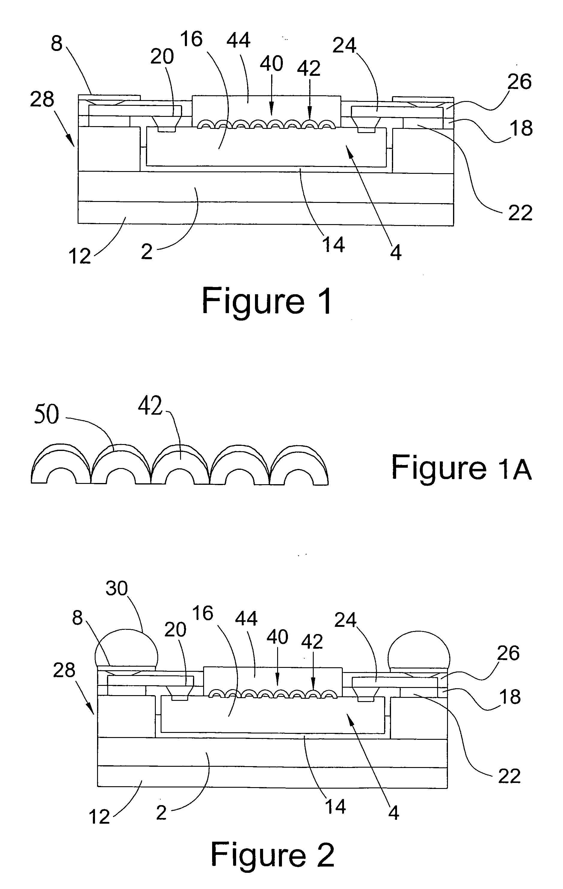
[0019]The present invention discloses a structure of WLP utilizing a cavity formed into the substrate. A photosensitive material is coated over the die and the pre-formed substrate. Preferably, the material of the photosensitive material is formed of the elastic material.

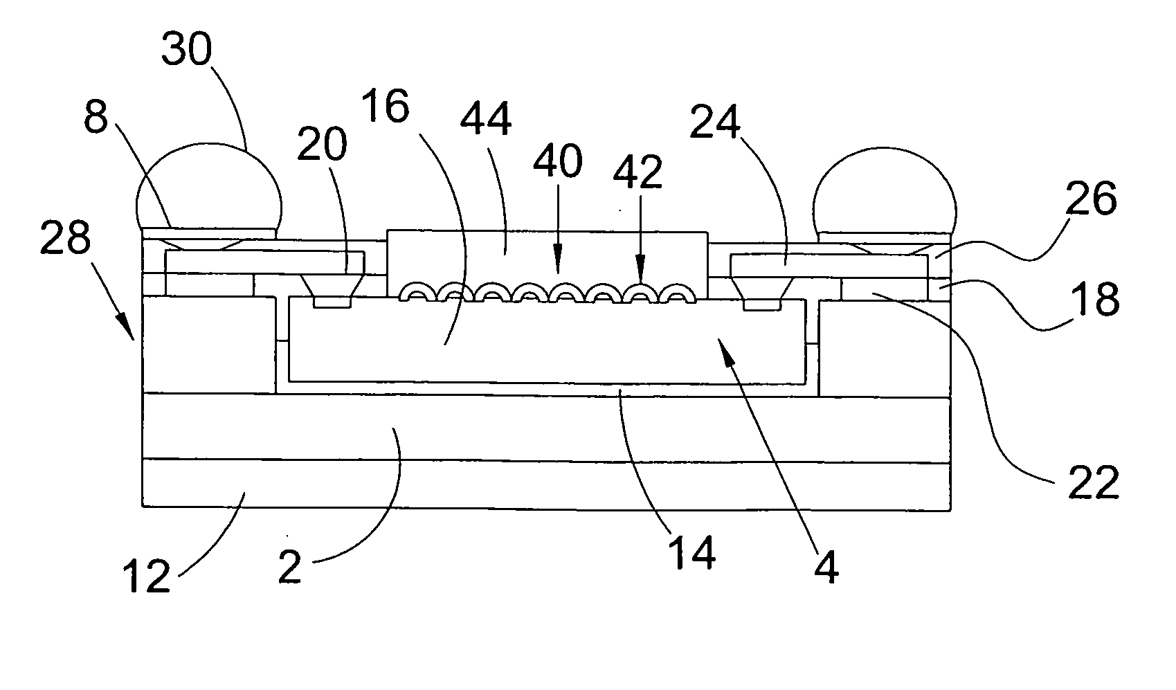
[0020]FIG. 1 illustrates a cross-sectional view of Fan-Out Wafer Level Package (FO-WLP) in accordance with one embodiment of the present invention. As shown in the FIG. 1, the structure of FO-WLP includes a substr...


PUM


Abstract

The present invention provides a structure of package comprising a substrate with a die receiving cavity formed within an upper layer of the substrate, wherein terminal pads are formed on the upper surface of the substrate, the same plain as the micro lens. A die is disposed within the die receiving cavity by adhesion and a dielectric layer formed on the die and the substrate. A re-distribution metal layer (RDL) is formed on the dielectric layer and coupled to the die. An opening is formed within the dielectric layer and a top protection layer to expose the micro lens area of the die for Image Sensor chip. A protection layer (film) be coated on the micro lens area with water repellent and oil repellent to away the particle contamination. A transparent cover with coated IR filter is optionally formed over the micron lens area for protection.

Description

CROSS REFERENCES TO THE RELATED APPLICATIONS[0001]This application is a divisional application of pending U.S. patent application Ser. No. 11 / 708,476, filed Feb. 21, 2007 (of which the entire disclosure of the pending, prior application is hereby incorporated by reference).FIELD OF THE INVENTION[0002]This invention relates to a structure of wafer level package (WLP), and more particularly to a carrier (substrate) with die receiving cavity to receive an Image Sensor die for WLP.DESCRIPTION OF THE PRIOR ART[0003]In the field of semiconductor devices, the device density is increased and the device dimension is reduced continuously. The demand for the packaging or interconnecting techniques in such high density devices is also increased to fit the situation mentioned above. Conventionally, in the flip-chip attachment method, an array of solder bumps is formed on the surface of the die. The formation of the solder bumps may be carried out by using a solder composite material through a so...

Claims


Application Information

Patent Timeline
Patent Type & Authority Applications(United States)
IPC IPC(8): H01L21/00
CPCH01L27/14618H01L27/14625H01L27/14683H01L27/14685H01L31/0203H01L2924/0002H01L31/0232H01L2924/00H01L31/02327
Inventor YANG, WEN-KUNCHANG, JUI-HSIENWANG, TUNG-CHUAN
Owner ADVANCED CHIP ENG TECH INC
Why Eureka
Try Eureka