Simple Adaptive Wavelet Thresholding

a wavelet thresholding and wavelet technology, applied in the field of digital imaging, can solve the problems of increasing noise, reducing size, and increasing the size of image sensors, and reducing the quality of image data

Inactive Publication Date: 2008-11-20
SEIKO EPSON CORP
View PDF16 Cites 14 Cited by
  • Summary
  • Abstract
  • Description
  • Claims
  • Application Information

AI Technical Summary

Benefits of technology

[0016]Broadly speaking, the present invention fills these needs by providing a digital imaging device and method providing digital filter effects.

Problems solved by technology

As imaging devices are reduced in size to fit in small form-factor electronics such as cell phones, manufacturers struggle to provide high quality, high-resolution, images using image sensors of increasingly smaller sizes.
As pixel sensor elements reduce in size, they collect less light, and therefore require greater amplification, which results in increased noise, particularly in darker environments.
In extreme cases, noise is observable in the overall image as a snowy or speckled effect, which is generally undesirable.
Typically, small battery-powered digital imaging devices such as video or still cameras, and devices incorporating such cameras, such as cell phones, personal digital assistants (PDAs), etc., lack the processor and memory requirements to add digital filter effects such as noise reduction.
Therefore, calculation of the threshold value according to the formula above would consume processor cycles and memory of limited power devices, which in turn would result in shortened battery life and inconvenience to the user, who would have to wait for the processing to complete before viewing or storing the resulting image.
The use of an arbitrary global threshold value provides adequate results for most purposes, but does not provide the best results in all parts of a specific image.

Method used


Image

  • Simple Adaptive Wavelet Thresholding
  • Simple Adaptive Wavelet Thresholding
  • Simple Adaptive Wavelet Thresholding

Examples


Embodiment Construction

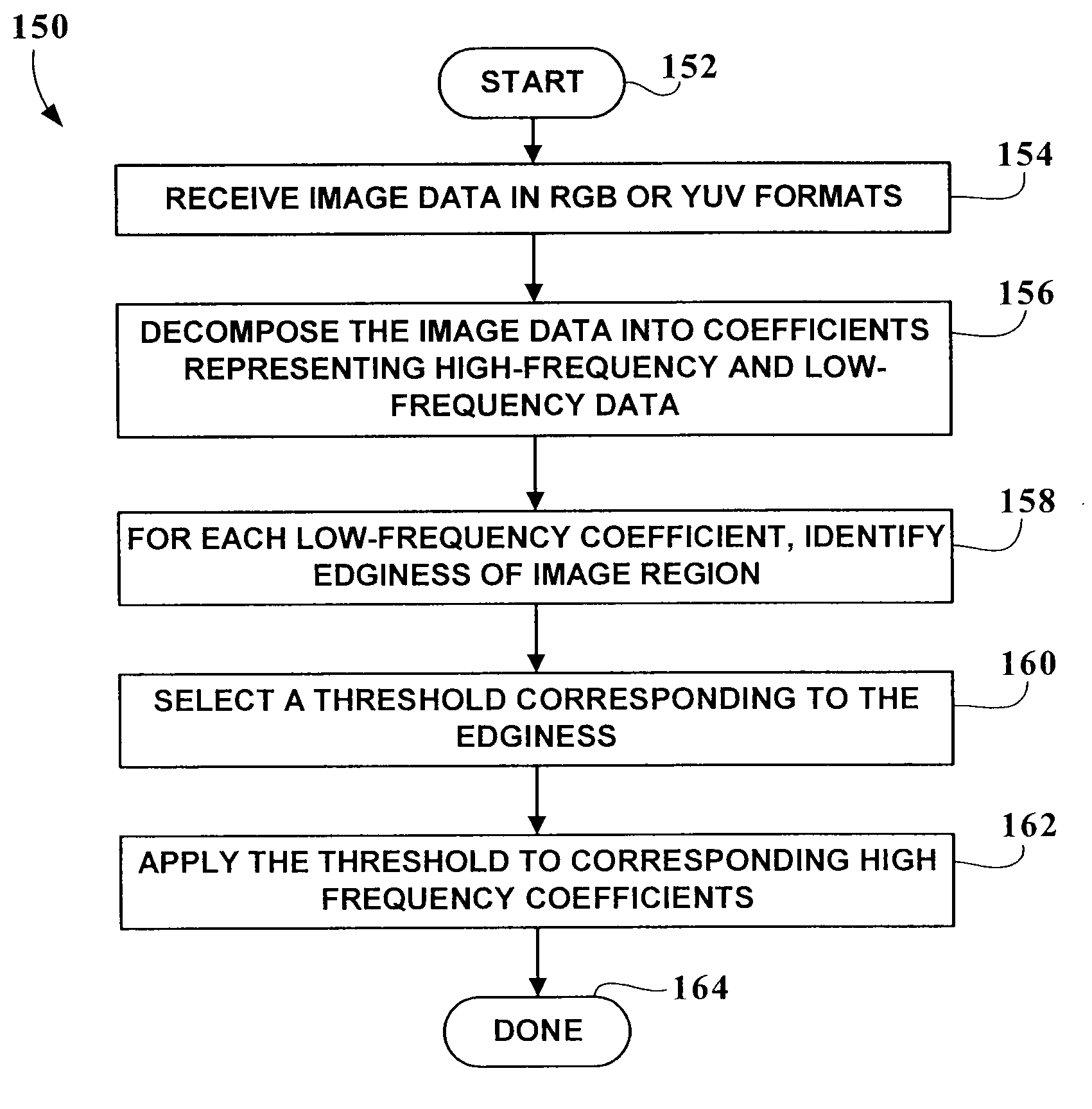
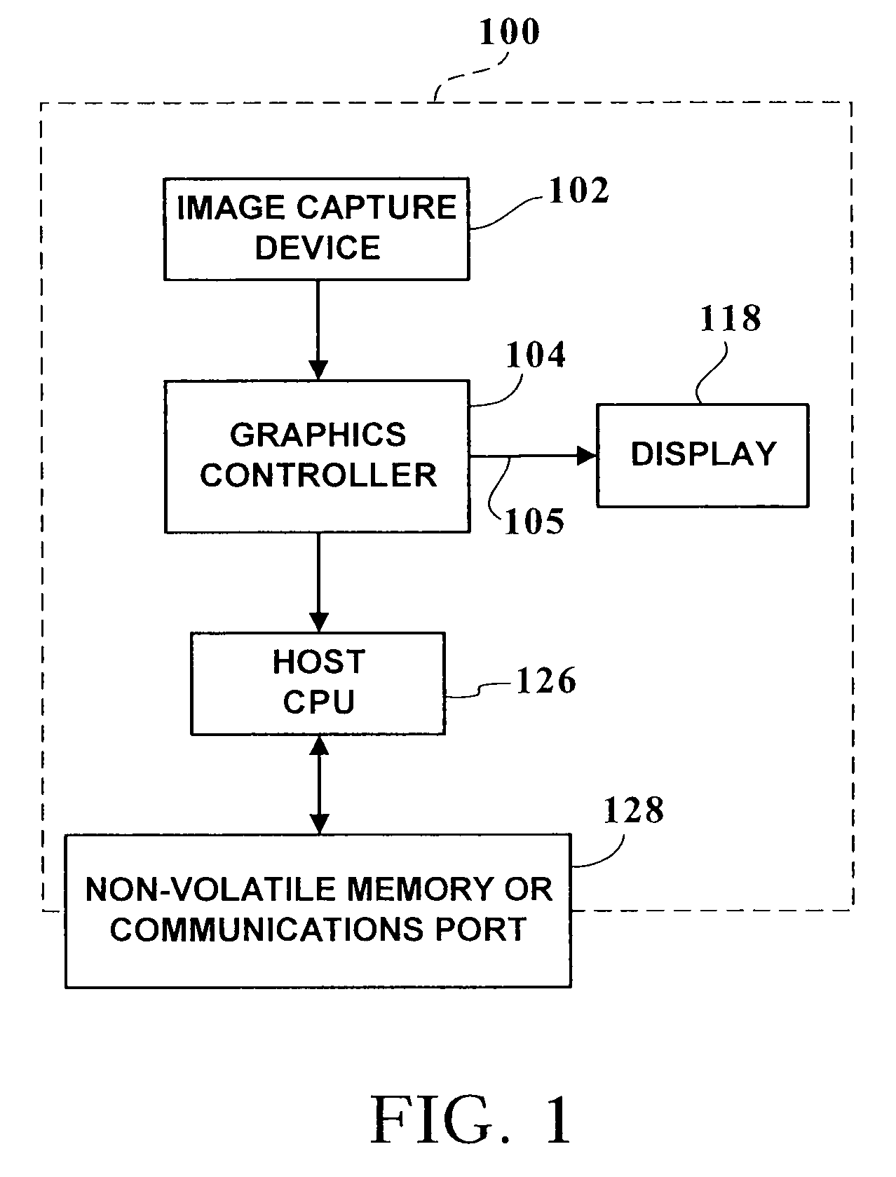
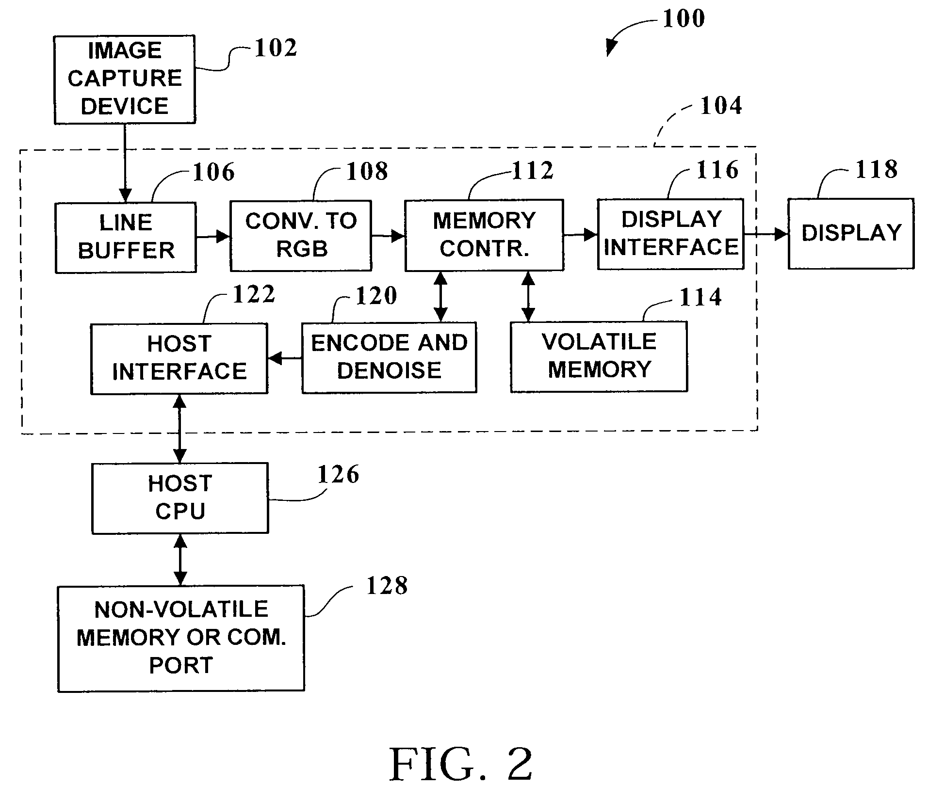
[0028]FIG. 1 shows a schematic overview of an imaging device 100. Imaging device 100 may be a digital camera, digital video recorder, or some electronic device incorporating a digital camera or video recorder, such as, for example, a personal digital assistant (PDA), cell phone or other communications device, etc. Imaging device 100 includes a graphics controller 104, a host central processing unit (CPU) 126, a display 118, and an image capture device 102. Graphics controller 104 provides an interface between display 118, host CPU 126, and image capture device 102.

[0029]The timing control signals and data lines, such as line 105 communicating between graphics controller 104 and display 118, are shown as a single line but may in fact be several address, data, and control lines and / or a bus. All communication lines shown in the figures will be presented in this manner to reduce the complexity and better present the novel aspects of the invention.

[0030]Host CPU 126 performs digital pro...


PUM


Abstract

A method for processing an image is described. In the method, image data representing an image into a memory device. The image data is filtered to obtain a plurality of coefficients representing low and high frequency image data. An area of low frequency data corresponding to one of the coefficients is analyzed to identify a degree of edginess of the region. A threshold is obtained, the threshold varying depending on the degree of edginess. If the coefficient is less than the threshold, it is reduced to zero. Wavelet-based image compression can then be performed on the image using the reduced coefficients.

Description

BACKGROUND OF THE INVENTION[0001]1. Field of the Invention[0002]The present invention relates generally to digital imaging. More particularly, the present invention relates to a method and device for wavelet-based compression of image data.[0003]2. Description of the Related Art[0004]As imaging devices are reduced in size to fit in small form-factor electronics such as cell phones, manufacturers struggle to provide high quality, high-resolution, images using image sensors of increasingly smaller sizes. As the overall size of an image sensor is reduced and the number of pixels increase, each single-pixel sensor element becomes smaller and smaller. A pixel sensor element is the portion of an image sensor that detects light for one pixel of an image. As pixel sensor elements reduce in size, they collect less light, and therefore require greater amplification, which results in increased noise, particularly in darker environments. A pixel sensor is referred to as “noisy” when the intensi...

Claims


Application Information

Patent Timeline
Patent Type & Authority Applications(United States)
IPC IPC(8): G06K9/36
CPCH04N19/176H04N19/63H04N19/122H04N19/117H04N19/59H04N19/14H04N19/18H04N19/17H04N19/635H04N19/132
Inventor RAI, BARINDER SINGHSONG, JILIANG
Owner SEIKO EPSON CORP
Why Eureka
Try Eureka