Semiconductor Storage Device and Burst Operation Method

a technology of semiconductors and storage devices, applied in the field of semiconductor memory and burst operation methods therefor, can solve the problems of difficult acceleration, low efficiency, and reduced external cycle time, and achieve the effect of increasing the burst length

Inactive Publication Date: 2008-11-27
SUNAGA TOSHIO +3
View PDF16 Cites 6 Cited by
  • Summary
  • Abstract
  • Description
  • Claims
  • Application Information

AI Technical Summary

Benefits of technology

[0006]It is an object of the present invention to provide a semiconductor memory in which a burst length can be increased without increasing consumed current and a burst operation method therefor.

Problems solved by technology

For this purpose, however, the internal cycle time needs to be reduced to less than one half of the external cycle time and thus the reduction of the external cycle time is not an easy matter.
Therefore, it can show only half of its performance and it is hard to achieve the acceleration.

Method used


Image

  • Semiconductor Storage Device and Burst Operation Method
  • Semiconductor Storage Device and Burst Operation Method
  • Semiconductor Storage Device and Burst Operation Method

Examples


Embodiment Construction

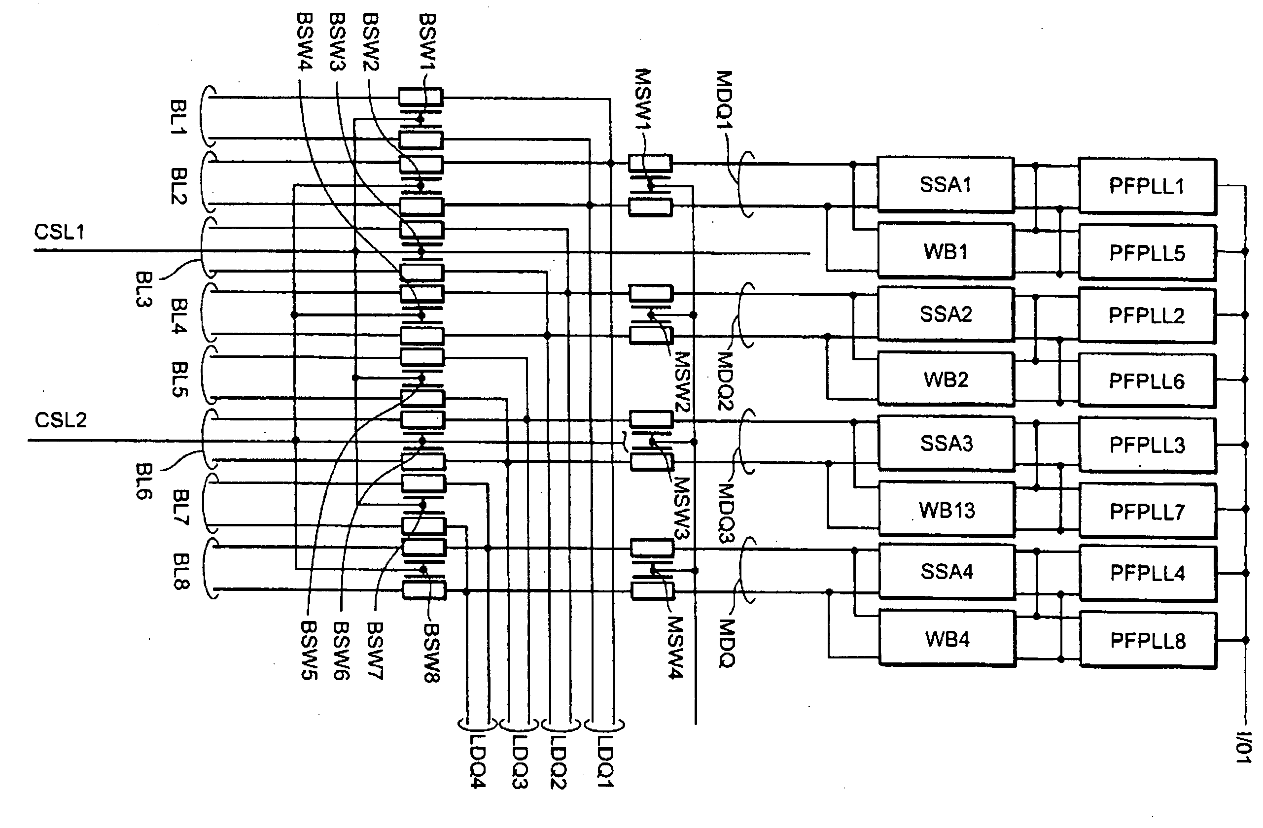
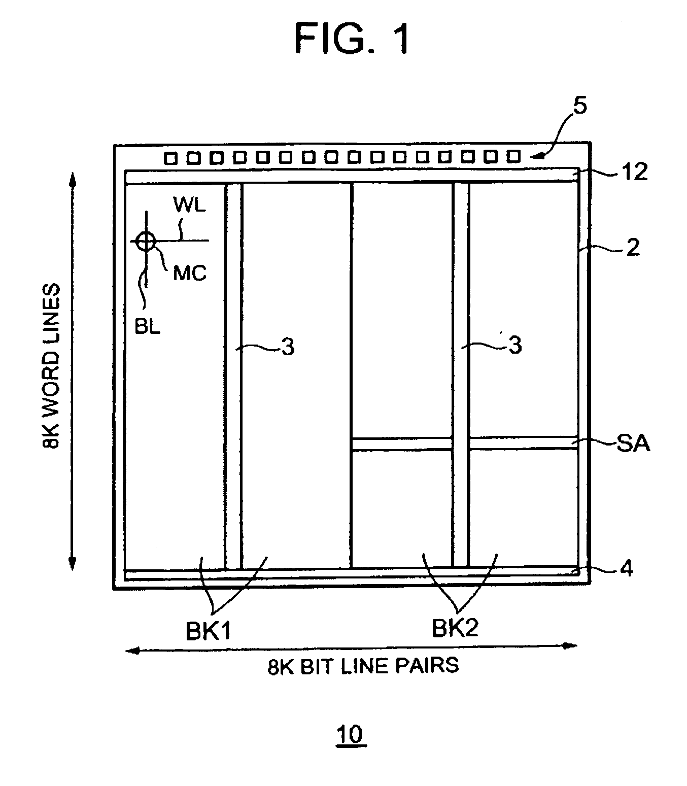
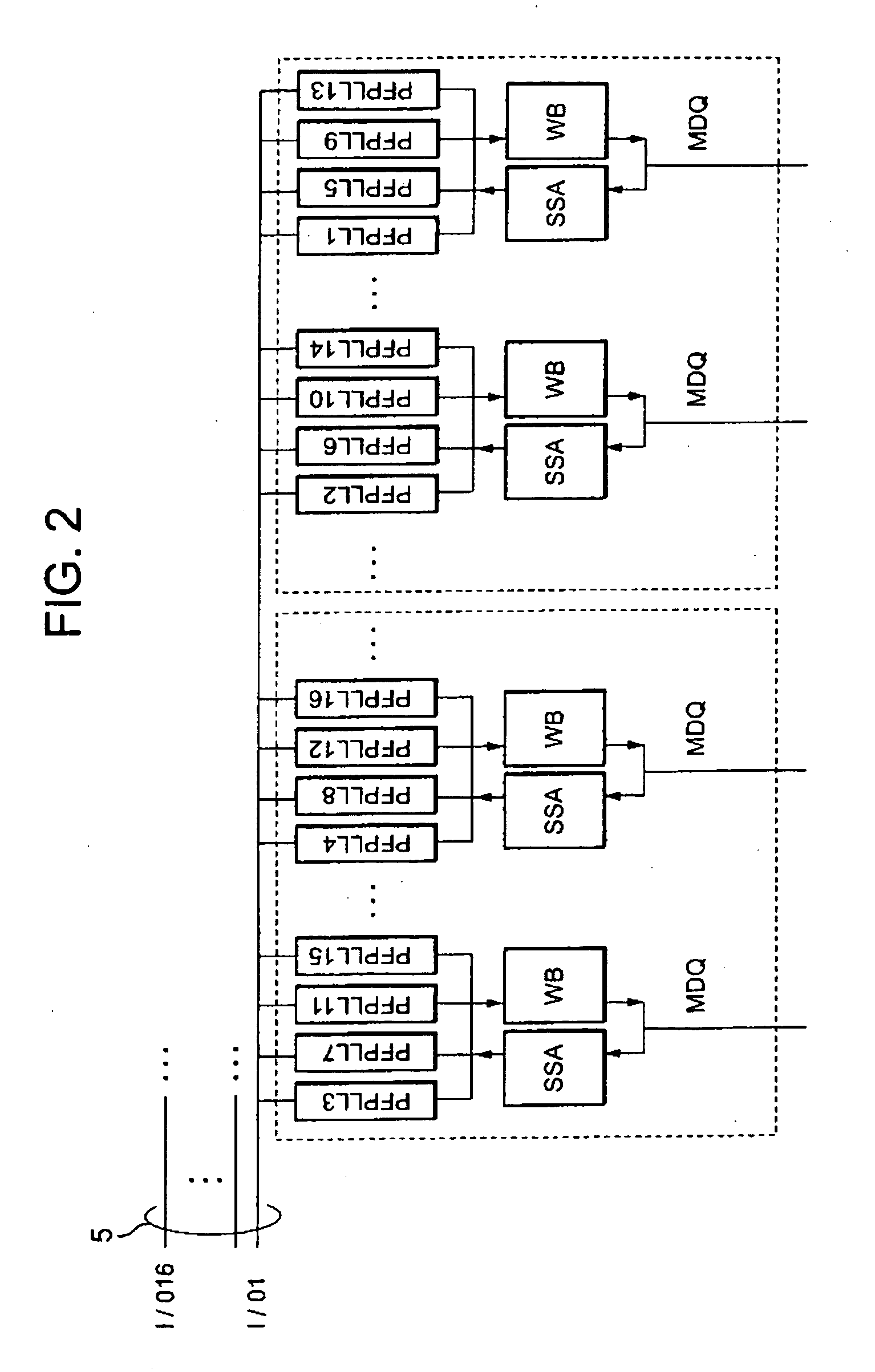
[0047]The semiconductor memory according to the present invention comprises data I / O buses, a plurality of latch circuits, a memory cell array, sense amplifier activating means, a column decoder, and control means. The plurality of latch circuits are connected in common to the data I / O bus. The memory cell array includes a plurality of bit line pairs, a plurality of bit switches, a plurality of column selection lines, and a plurality of sense amplifiers. The plurality of bit switches are connected between the plurality of latch circuits and the plurality of bit line pairs and divided into a plurality of groups. The plurality of column selection lines are provided so as to correspond to the plurality of groups. Each column selection line is connected to a plurality of bit switches included in the corresponding group. The plurality of sense amplifiers are connected to the plurality of bit line pairs. The sense amplifier activating means activates the sense amplifiers. The column decod...


PUM


Abstract

The present invention is a PSRAM in which a burst length can be increased without increasing consumed current, and a burst operation method therefor. In operation, column selection lines CSL1 and CSL2 are driven in order during activation of sense amplifiers. This causes bit switches BSW1-BSW8 to be turned on in units of four bit switches and then 8-bit read data RD is latched from bit line pairs BL1-BL8 into prefetch/preload latches PFPLL1-PFPLL8 in units of 4-bits. The 8-bit read data RD is continuously output to a single data I/O bus I/O1 in units of one bit and in order.

Description

CROSS REFERENCE TO RELATED APPLICATIONS[0001]This application is based on PCT application No. PCT / JP2004 / 16296, filed Nov. 4, 2004 which claims priority to Japanese Patent Application 2003-377485, filed Nov. 6, 2003, now abandoned, herein incorporated by reference.BACKGROUND OF THE INVENTION[0002]1. Field of the Invention[0003]The present invention relates to a semiconductor memory and a burst operation method therefor, and more particularly to an improvement of a dynamic random accesses memory (DRAM) capable of inserting a refresh operation during a normal access operation and a burst operation method therefor.[0004]2. Background of the Invention[0005]In recent years, it has become popular to replace a static random accesses memory (SRAM) with a DRAM for uses in low power consumption. It is because a storage capacity per unit area of the DRAM is much larger than that of the SRAM. The DRAM, however, needs a refresh, which is unnecessary for the SRAM. Therefore, what is needed is a p...

Claims


Application Information

Patent Timeline
Patent Type & Authority Applications(United States)
IPC IPC(8): G11C7/00G11C8/00G11C7/08G11C7/10G11C11/4096
CPCG11C7/08G11C7/1018G11C11/4076G11C11/4096G11C11/34G11C11/4091
Inventor SUNAGA, TOSHIOHOSOKAWA, KOHJIMIYATAKE, HISATADANAKAMURA, YUTAKA
Owner SUNAGA TOSHIO
Why Eureka
Try Eureka