Optical sensor and image forming apparatus including same

an image forming apparatus and optical sensor technology, applied in the direction of optical radiation measurement, photometry using electric radiation detectors, instruments, etc., can solve the problems of inability to calibrate, weakened specular light intensity, and fluctuation of analog output value, so as to achieve stable output value for calibration and enhance reliability of sensitivity calibration

Inactive Publication Date: 2008-11-27
RICOH KK
View PDF1 Cites 57 Cited by
  • Summary
  • Abstract
  • Description
  • Claims
  • Application Information

AI Technical Summary

Benefits of technology

[0027]In view of the foregoing, exemplary embodiments of the present invention provide an optical sensor capable of

Problems solved by technology

Calibration is needed because the amount of light of the light emitting element (for example, LED) may fluctuate over time due to deterioration of the, causing an analogue output value to fluctuate.
As a result, however, the intensity of the specular light is weakened.
On the other hand, in the sensor using the diffusely reflected light, the output value may be approximately zero relative to the surface of the toner image bearing member, making calibration impossible.
However, when an output voltage is almost zero, it is hardly possible to adjust the intensity of light emission of the light emitting element.
However, such an arrangement increases a data processing load.
However, disposing the reflecting plate on the surface of the toner image bearing member may disrupt image formation.
However, because the calibratio

Method used


Image

  • Optical sensor and image forming apparatus including same
  • Optical sensor and image forming apparatus including same
  • Optical sensor and image forming apparatus including same

Examples


exemplary embodiment 1

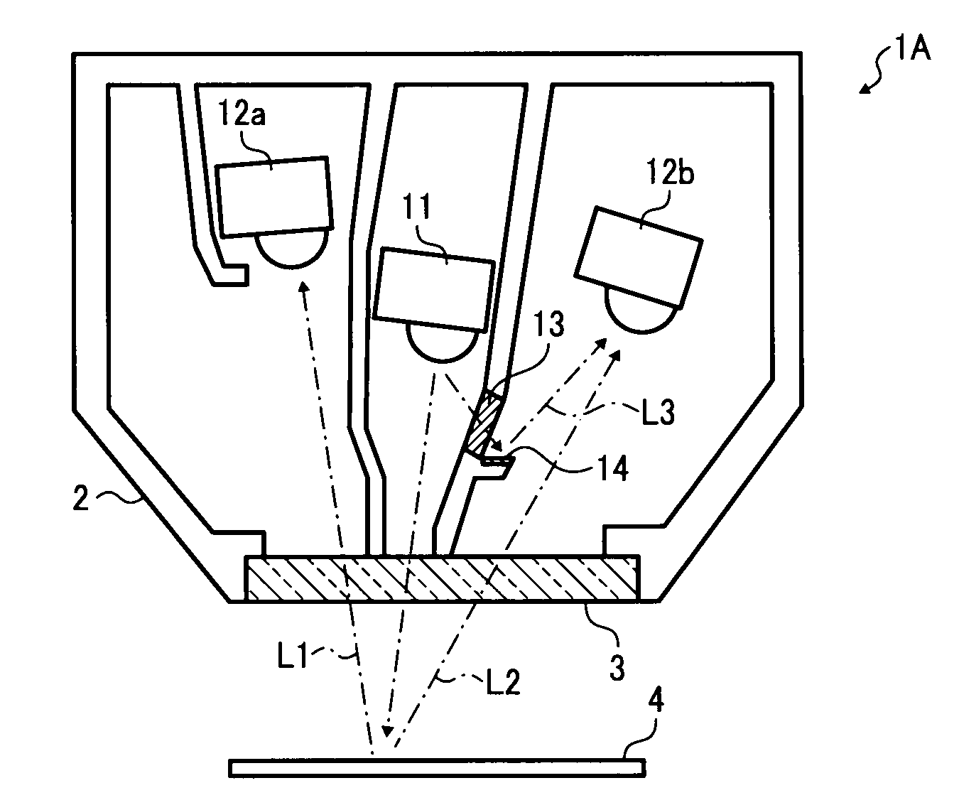
[0047]FIGS. 1A and 1B are cross-sectional views illustrating an optical sensor according to one exemplary embodiment of the present invention. The optical sensor illustrated in FIGS. 1A and 1B includes an optical function element disposed in a calibration optical path, switchable between a light permeating state, in which light is allowed to pass through, and a light intercepting state, in which light is blocked, when voltage is applied. In an image forming apparatus using dry toner, the optical sensor for detecting image information, particularly a color image forming apparatus, is most likely configured to detect both the specularly reflected light and the diffusely reflected light.

[0048]An optical sensor 1A illustrated in FIG. 1A includes at least one light emitting element 11 (normally, a light emitting diode (LED)) and two light receiving elements 12a and 12b (photodiodes or phototransistors), disposed within a sensor housing 2. The optical sensor 1A also includes a dust-proof ...

exemplary embodiment 2

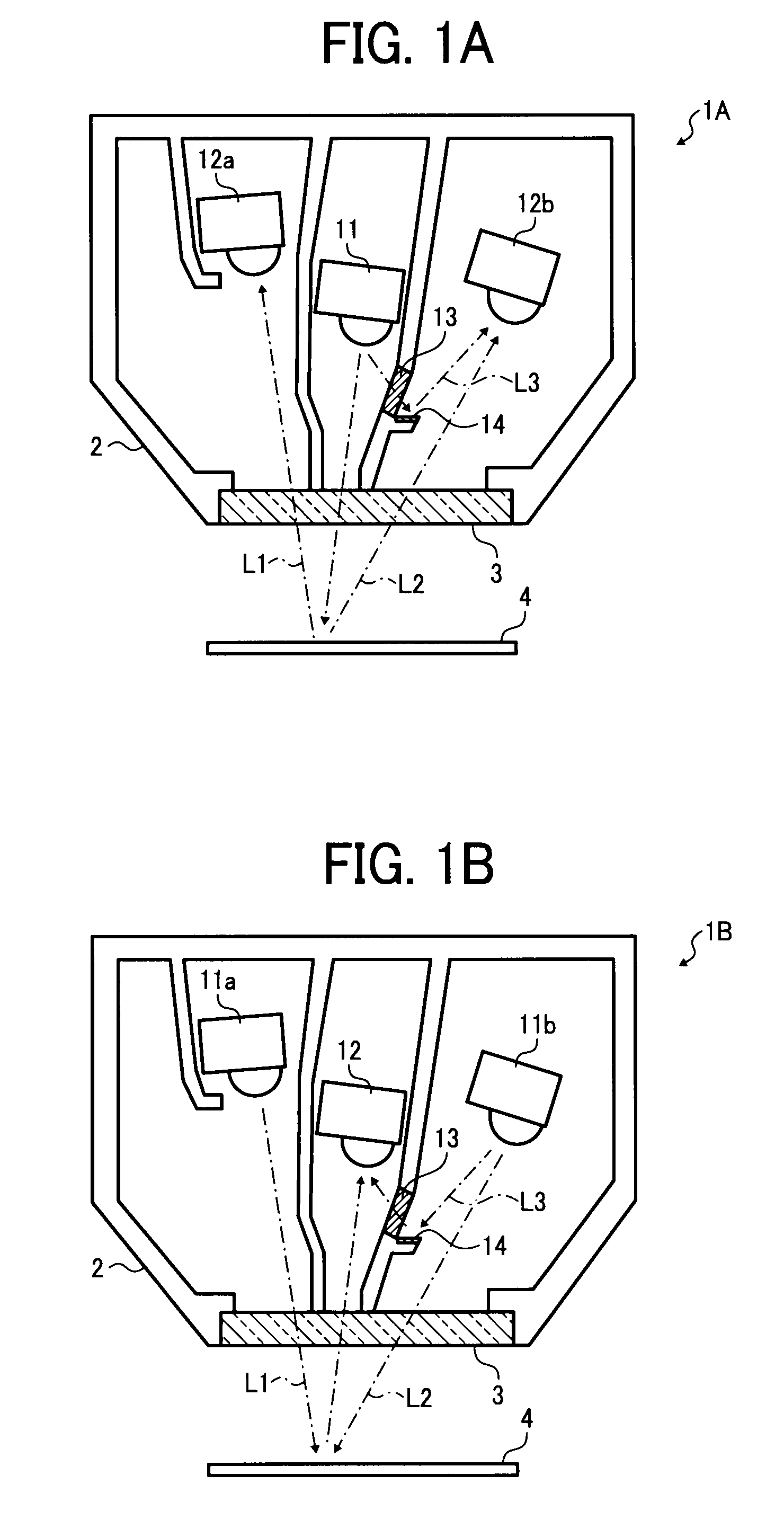
[0061]Referring now to FIG. 2, there is provided a cross-sectional view illustrating another exemplary embodiment of the present invention. FIG. 2 illustrates a second example of an optical sensor including an optical function element 15 disposed in front of the calibration reflecting plate 14. The optical function element 15 is switchable between the light permeating state and the light intercepting state when voltage is applied.

[0062]The structure of an optical sensor 1C in FIG. 2 is similar if not identical to, that of the optical sensor 1A illustrated in FIG. 1A. However, according to the second exemplary embodiment, the second optical function element 15 is provided in front of the calibration reflecting plate 14 illustrated in FIG. 1A. Similar to the optical function element 13 illustrated in FIG. 1A, the optical function element 15 may be formed of a liquid crystal element.

[0063]When calibration is performed in the optical sensor 1C, the state of both the optical function ele...

exemplary embodiment 3

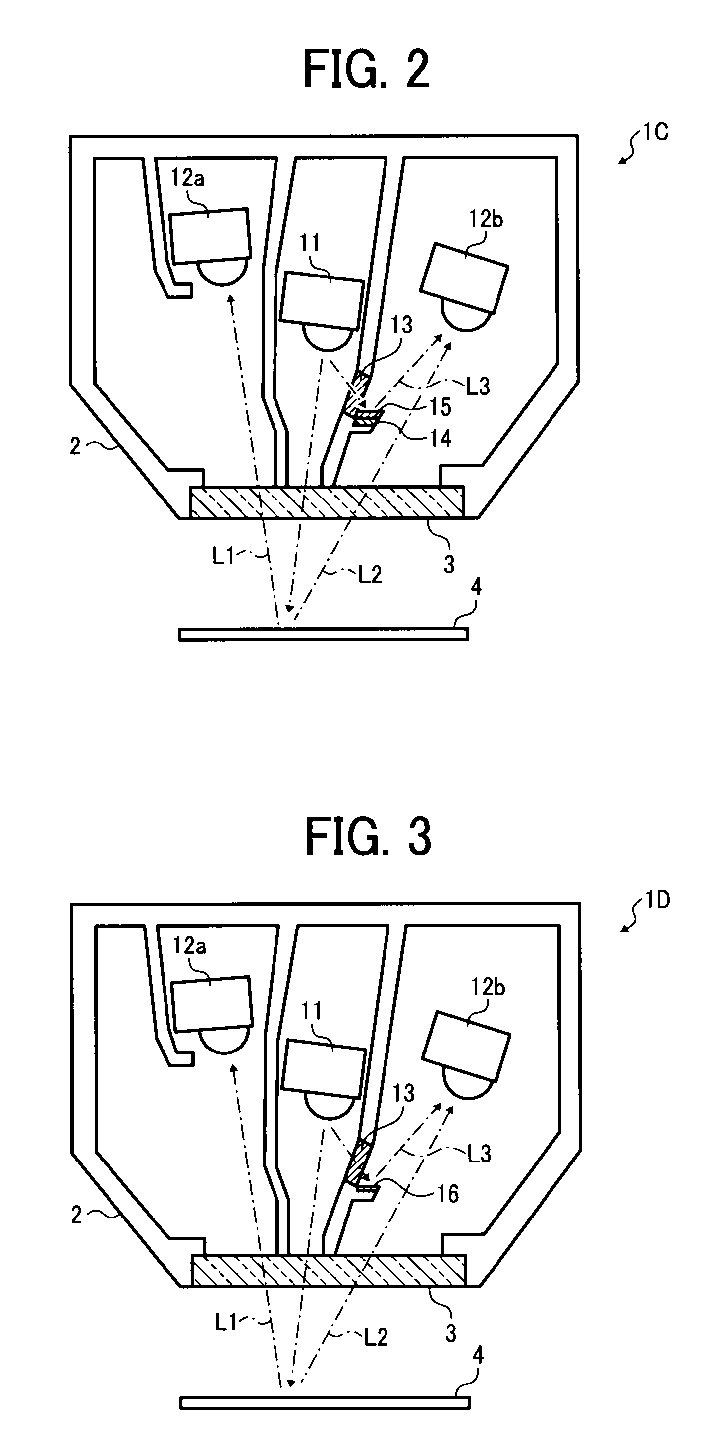
[0068]Referring now to FIG. 3, there is provided a cross-sectional view illustrating still another exemplary embodiment of the present invention. FIG. 3 illustrates a third example of an optical sensor including an optical function element 16 serving as a reflecting plate for calibration. The optical function element 16 is switchable between the light permeating state and the light intercepting state when voltage is applied.

[0069]The structure of an optical sensor 1D is similar if not identical to, that of the optical sensor 1A illustrated in FIG. 1A. However, according to the exemplary embodiment, a white reference plate which is typical of a reflecting plate is not used. Instead, the optical function element 16 switchable between the light permeating state and the light intercepting state is provided. The optical function element 16 having such functions includes a light control mirror material developed by National Institute of Advanced Industrial and Technology, for example.

[007...


PUM


Abstract

An optical sensor includes a light-emitting element for directing light to an image, a light-receiving element for receiving light reflected by the image, a normal detection optical path for allowing the light emitted by the light-emitting element and the light reflected from the image to follow a normal detection optical path during normal operation, a calibration reflecting plate disposed inside the optical sensor for reflecting light from the light-emitting element when sensitivity is calibrated, a calibration optical path for allowing the light emitted by the light-emitting element to follow a calibration optical path to the light-receiving element when the emitted light is reflected by the calibration reflecting plate, and a first optical function element disposed in the calibration optical path and switchable between a light permeating state, in which the light passes therethrough, and a light intercepting state, in which the light is blocked, when voltage is applied.

Description

CROSS-REFERENCE TO RELATED APPLICATIONS[0001]This patent application is based on and claims priority pursuant to 35 U.S.C. §119 from Japanese Patent Application No. 2007-133899 filed on May 21, 2007 in the Japan Patent Office, the entire contents of which is hereby incorporated herein by reference.BACKGROUND OF THE INVENTION[0002]1. Field of the Invention[0003]Exemplary aspects of the present invention generally relate to an optical sensor and an electrophotographic image forming apparatus using the same, and more particularly, to an optical sensor for detecting image information and an electrophotographic image forming apparatus, such as a copier, a printer, a facsimile, and a multi-function machine, using the same.[0004]2. Description of the Background Art[0005]Various types of optical sensors for detecting image information used in an electrophotographic image forming apparatus using dry toner, and technologies relating to the image forming apparatus equipped with such an optical...

Claims


Application Information

Patent Timeline
IPC IPC(8): G01J1/20G03G15/04
CPCG01J1/0271G01N21/55G01J1/0403G01J1/0414G01J1/044G01J1/08G01J1/4223G01J1/4228G01J2001/4233G01N21/276G03G2215/00042G03G2215/00059G03G15/0131G03G15/5041G03G15/5058G01J1/04
Inventor HIRAI, SHUJI
Owner RICOH KK
Why Eureka
Try Eureka