

Light-emitting device
a technology of light-emitting devices and light-emitting components, which is applied in the direction of semiconductor devices, basic electric elements, electrical equipment, etc., can solve the problems of increasing cost, increasing complexity of production, and reducing production efficiency
- Summary
- Abstract
- Description
- Claims
- Application Information
AI Technical Summary
Benefits of technology
Problems solved by technology
Method used
Image

Examples
first embodiment
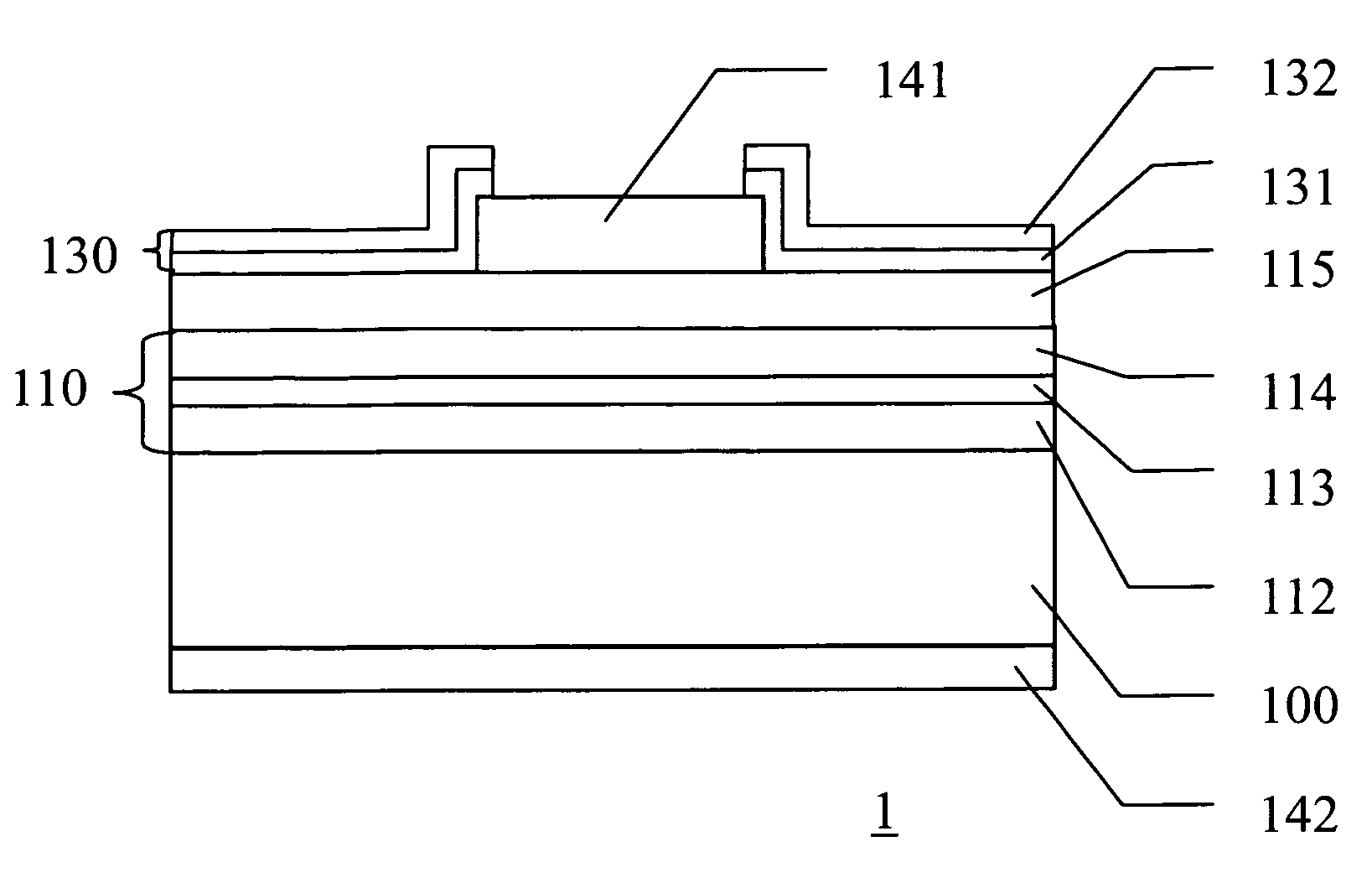
[0022]Referring to FIG. 1, the schematic cross-sectional view shows a light-emitting device 1 in accordance with the present invention. The light-emitting device 1 such as an LED comprises a substrate 100, a semiconductor light-emitting stack 110, an optical field tuning layer 130, and upper and lower electrodes 141 and 142. The material of the substrate 100 includes III-V semiconductor material such as GaAsP, GaAs, or GaP. The semiconductor light-emitting stack 110 formed on the substrate 100 includes an n-type semiconductor layer 112, a p-type semiconductor layer 114, an active layer interposed therebetween, and a second p-type semiconductor layer 115. In some embodiments, the arrangements of the n-type and p-type semiconductor layers 112 and 114 can be interchanged, and the second p-type semiconductor layer 115 can be replaced by a second n-type semiconductor layer. In the embodiment, the n-type and p-type semiconductor layers 112 and 114 act as cladding layers of the LED and inc...
second embodiment
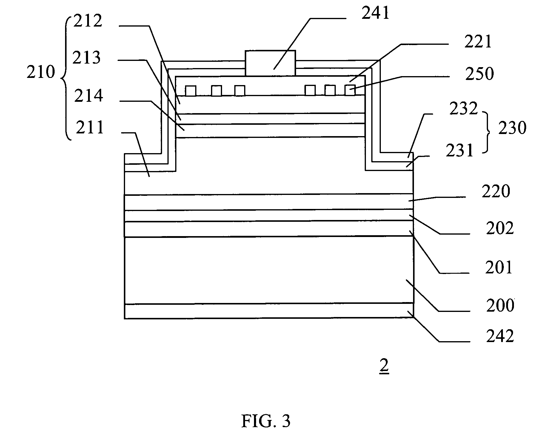
[0028]Referring to FIG. 3, the schematic cross-sectional view shows a light-emitting device 2 in accordance with the present invention. The light-emitting device 2 includes a substrate 200, a conductive adhesive layer 201, a reflective layer 202, a first transparent conductive oxide layer 220, a semiconductor light-emitting stack 210, a distributed contact layer 250, a second transparent conductive oxide layer 221, an optical field tuning layer 230, and upper and lower electrodes 241 and 242. The material of the substrate 200 includes but is not limited to Si, GaAs, metal or other similar materials. The conductive adhesive layer 201 is formed on the substrate 200, and a first bonding interface is formed therebetween. The material of the conductive adhesive layer 201 includes but is not limited to Ag, Au, Al, In, spontaneous conductive polymer, or polymer doping with metal like Al, Au, Pt, Zn, Ag, Ni, Ge, In, Sn, Ti, Pb, Cu, Pd, or other metals. The reflective layer 202 is formed on ...
third embodiment
[0031]Referring to FIG. 5, the schematic cross-sectional view shows a light-emitting device 3 in accordance with the present invention. The structure of the light-emitting device 3 is similar to the light emitting device 2, and the difference is the light emitting device 3 does not include the second transparent conductive oxide layer 221 and the distributed contact layer 250. The n-type semiconductor 212 of the light emitting device 3 includes a roughened top surface. The roughened top surface can be formed during the epitaxial process or by a randomly etching method to form a multi-cavity surface. It also can be formed by a lithographical etching to form a regular or an irregular patterned surface. The n-type semiconductor 212 also includes an even top surface, and an upper electrode 340 is formed on the even top surface. The even top surface can form an ohmic contact with the upper electrode 340. The upper electrode 340 includes a bonding electrode 3401 and an extension electrode...
PUM
 Abstract
Description
Claims
Application Information