

Highly Scalable Thin Film Transistor
- Summary
- Abstract
- Description
- Claims
- Application Information
AI Technical Summary
Benefits of technology
Problems solved by technology
Method used
Image

Examples
first example
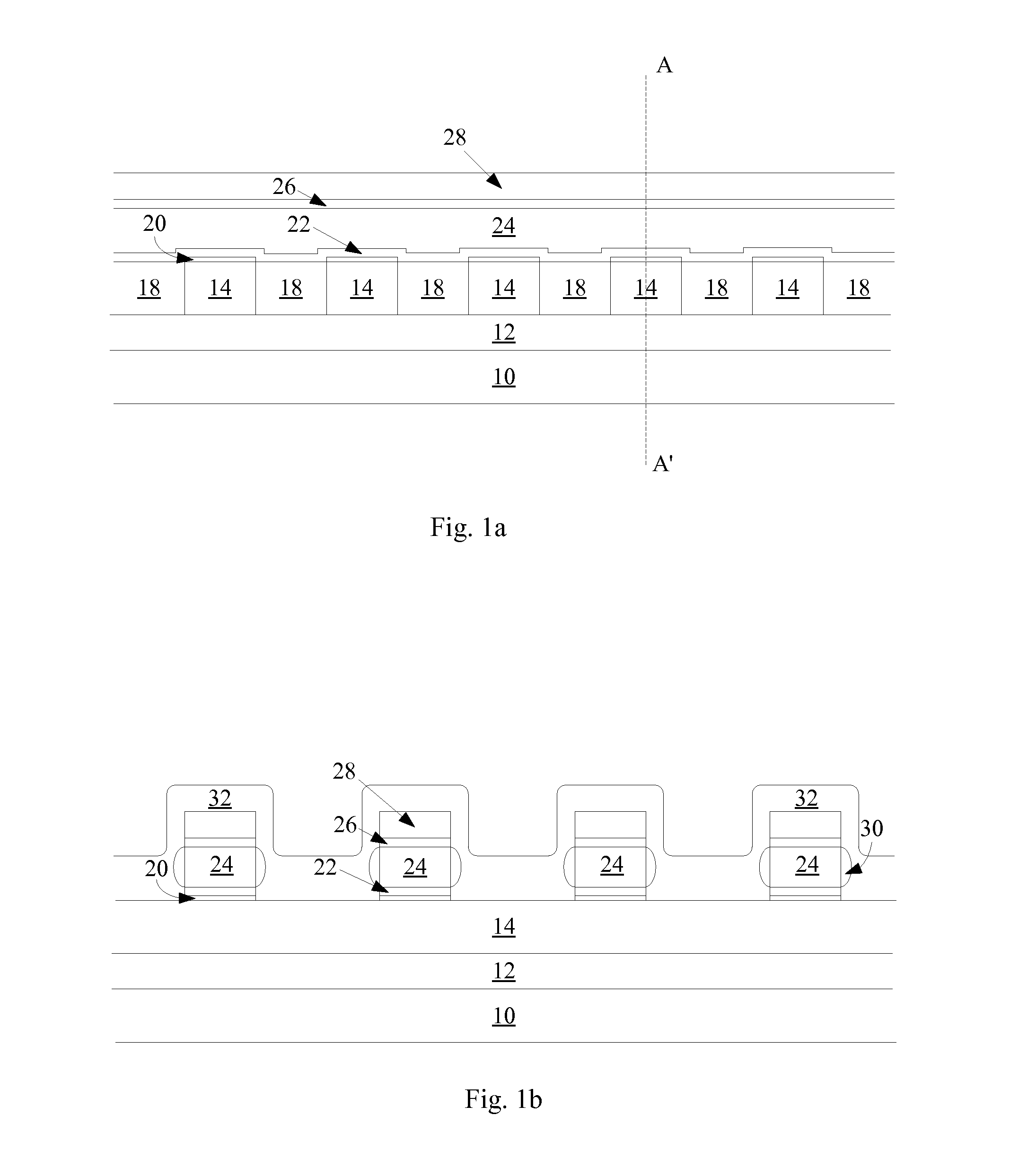
[0025]Fabrication begins on a suitable substrate. Turning to FIG. 1a, in some embodiments, substrate 10 may be a monocrystalline semiconductor substrate, for example a conventional silicon wafer. Control circuitry can be fabricated in the wafer substrate before fabrication of devices above the wafer begins. Alternatively, any other suitable substrate may be used, such as glass. Insulating layer 12 may be formed above substrate 10.
[0026]Channel layer 14 is deposited on insulating layer 12 by any conventional method, for example by chemical vapor deposition (CVD). Channel layer 14 is a semiconductor material, for example silicon, germanium, or silicon-germanium. In preferred embodiments, channel layer 14 is silicon-germanium, preferably between about 10 and about 40 atomic percent germanium, for example between about 10 and about 30 atomic percent germanium. In one embodiment, channel layer 14 is about 20 atomic percent germanium. Stated another way, channel layer 14 is SixGe1-x, wher...
second example
[0044]A second example will be provided of an embodiment of the present invention. In the second example, a charge storage element is formed between the channel region and the control gate, forming a charge storage memory cell.
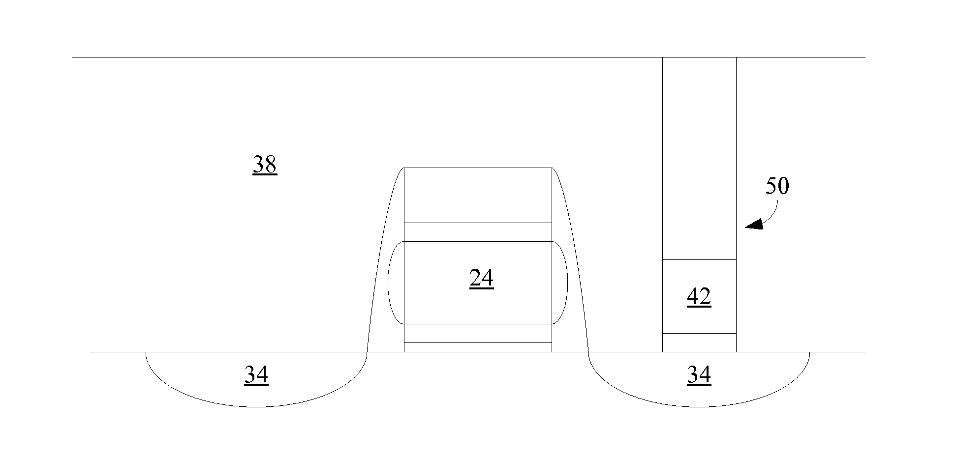
[0045]Turning to FIG. 3, fabrication begins as in the first example, with channel stripes 14 and dielectric material 18 formed above substrate 10 and dielectric 12, and exposed at a planar surface, for example by CMP. Channel stripes 14 may be formed of the same semiconductor materials named in the prior example, such as silicon-germanium. The view of FIG. 3 is in the same orientation as the view of FIG. 1b, viewing channel stripe 14 in cross-section extending left-to-right across the page.
[0046]Tunneling dielectric 41 is formed on this planar surface. This layer is preferably a thin, high-quality dielectric which will allow Fowler-Nordheim tunneling while the memory cell is being programmed and erased, but will prevent loss of charge in a programmed cell. In ...
PUM
 Abstract
Description
Claims
Application Information