Transformation of an input signal into a logical output voltage level with a hysteresis behavior

a technology of logical output voltage and input signal, applied in logic circuits, logic circuit coupling/interface arrangements, pulse techniques, etc., can solve the problems of digital switching circuit to transition to a different, multiple trigger circuits, etc., and achieve the effect of improving hysteresis behavior

Inactive Publication Date: 2009-01-08
NXP BV
View PDF7 Cites 12 Cited by
  • Summary
  • Abstract
  • Description
  • Claims
  • Application Information

AI Technical Summary

Benefits of technology

[0004]There may be a need for a circuit and a method for transforming an input signal into a log...

Problems solved by technology

For example, an input digital signal to a digital switching circuit that contains noise may cause the digital switching circuit to transition to a different state due to the noise and not due to the informational content of the signal.
Howe...

Method used


Image

  • Transformation of an input signal into a logical output voltage level with a hysteresis behavior
  • Transformation of an input signal into a logical output voltage level with a hysteresis behavior
  • Transformation of an input signal into a logical output voltage level with a hysteresis behavior

Examples


Embodiment Construction

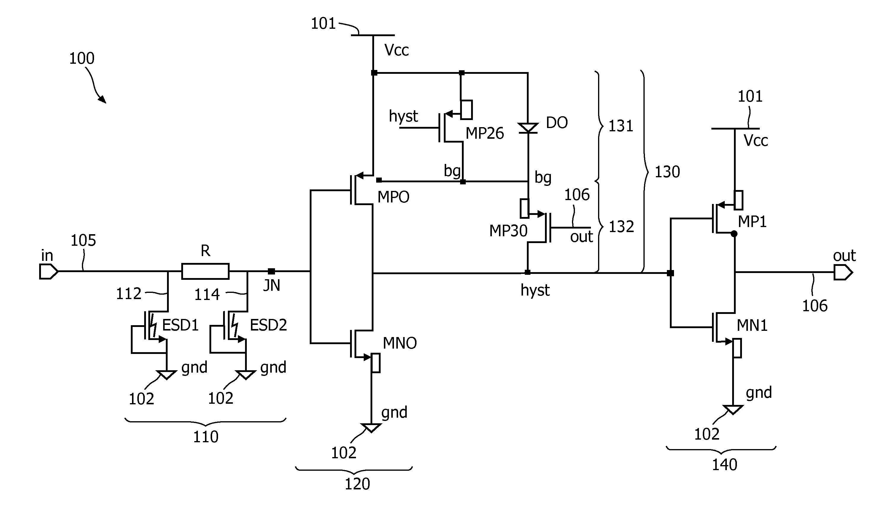
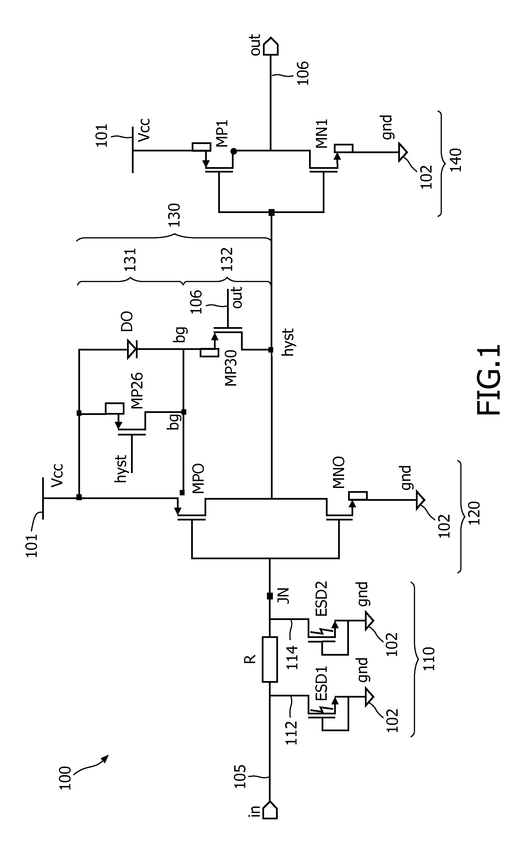
[0048]FIG. 1 shows a circuit diagram representing an electronic circuit arrangement 100 for transforming an input signal into a logical output voltage level. Since the circuit arrangement 100 may be used as an input stage for a variety of different logic devices the circuit arrangement 100 is also called an input cell.

[0049]The input cell 100 comprises a first conductor 101 providing an operating voltage Vcc. The input cell 100 further comprises a second conductor 102 providing a reference voltage, which according to the embodiment described here, is at ground level gnd. Although the two conductors 101 and 102 are not depicted as continuous conductor paths, each part of the two conductors 101 and 102 shown in FIG. 1 is electrically connected with other parts belonging to the same conductor, respectively.

[0050]The circuit arrangement 100 is subdivided into different circuit portions. Following an input terminal 105 representing a leadoff input node in, there is arranged an ESD protec...


PUM


Abstract

It is described a circuit and a method for transforming an input signal into a logical output. The circuit (100) comprises an inverter stage (120), connected in between the first conductor (101) and the second conductor (102). The inverter stage (120) includes a MOS switch (MP0), which comprises a first terminal being connected to the first conductor (101), a second terminal being connected to an output node (hyst), a gate terminal being connected to an input node (JN), and a back gate terminal. The circuit (100) further comprises a voltage divider (130), connected in between the first conductor (101) and the output node (hyst), wherein the voltage divider (130) provides a divider output node (bg) being connected to the back gate terminal. The circuit (100) represents an input cell having an improved hysteresis behavior over the total operating voltage range. This is achieved by adjusting the back gate voltage of the MOS switch (MP0) during a transition from an input level Low to an input level High. This causes a temporarily increased threshold voltage for turning off the MOS switch (MP0) during the transition.

Description

FIELD OF THE INVENTION[0001]The present invention relates to the field of electronic circuits, which perform a signal transformation from an input signal representing an input voltage level into a logical output voltage level. In particular, the present invention relates to such electronic circuits wherein the logical output voltage level comprises a hysteresis behavior when the input signal performs a sweeping change within a voltage range representing a plurality of possible input voltage levels.BACKGROUND OF THE INVENTION[0002]In designing digital circuits and systems, noise immunity and stability, are important criteria. For example, an input digital signal to a digital switching circuit that contains noise may cause the digital switching circuit to transition to a different state due to the noise and not due to the informational content of the signal. To prevent multiple triggering of the digital circuit and to provide noise immunity, digital switching circuits often employ a h...

Claims


Application Information

Patent Timeline
IPC IPC(8): H03K19/0185H03K19/00
CPCH03K19/0027H03K2217/0018H03K19/018521
Inventor HUITSING, ALBERT JANHOEFNAGEL, LOUWJANS, THIERRY
Owner NXP BV
Why Eureka
Try Eureka