
Method for producing display device and display device

a display device and display device technology, applied in the manufacture of electrode systems, cold cathode manufacturing, electric discharge tube/lamp manufacture, etc., can solve the problems of affecting the operation of the device, the sealing substrate or the terminal area, and the inability to completely remove the protective member, so as to achieve the effect of easy removal

Inactive Publication Date: 2009-01-08
SONY CORP
View PDF6 Cites 8 Cited by
  • Summary
  • Abstract
  • Description
  • Claims
  • Application Information

AI Technical Summary

Benefits of technology

[0012]The foregoing method for producing the display device is characterized in that the pseudo terminal areas corresponding to the terminal areas are formed between the separate positions where the terminal areas are formed. The term “corresponding” means that the pseudo terminal areas are identical with the terminal areas in their shape. In other words, they have approximately the same film thickness. Therefore, even though terminal areas are arranged separately, the protective member uniformly covers the terminal areas and the pseudo terminal areas by the existence of the pseudo terminal areas. The result is that the protective member can be removed easily without troubles mentioned above.
[0013]The display device according to an embodiment of the present invention has the pseudo terminal areas between the terminal areas. This structure permits the protective member to cover them uniformly and to be removed easily without troubles. Therefore, the protective member can be removed (or peeled off from the element substrate) adequately even though the terminal areas are arranged at separate positions as in the case of organic EL display devices of top emission type in complete solid sealed type.

Problems solved by technology

Unfortunately, the step of removing the protective member and exposing the terminal area has the disadvantage of chipping the sealing substrate or the terminal area or being unable to remove the protective member completely.
In such a case, depending on whether or not the terminal areas are arranged in place, the above-mentioned troubles with the removal of the protective member are liable to occur in an organic EL display device having a large screen.

Method used


Image

  • Method for producing display device and display device
  • Method for producing display device and display device
  • Method for producing display device and display device

Examples


Embodiment Construction

[0018]The following description referring to the accompanying drawings is a detailed description of the display device and the method for production thereof according to the present invention.

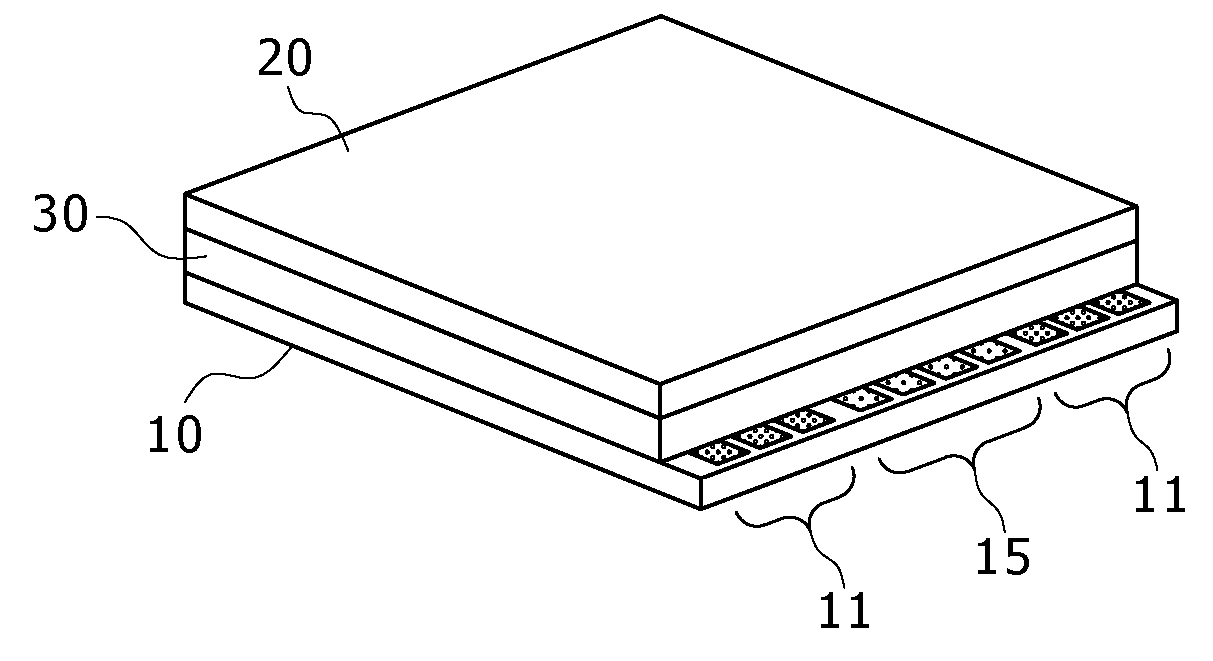
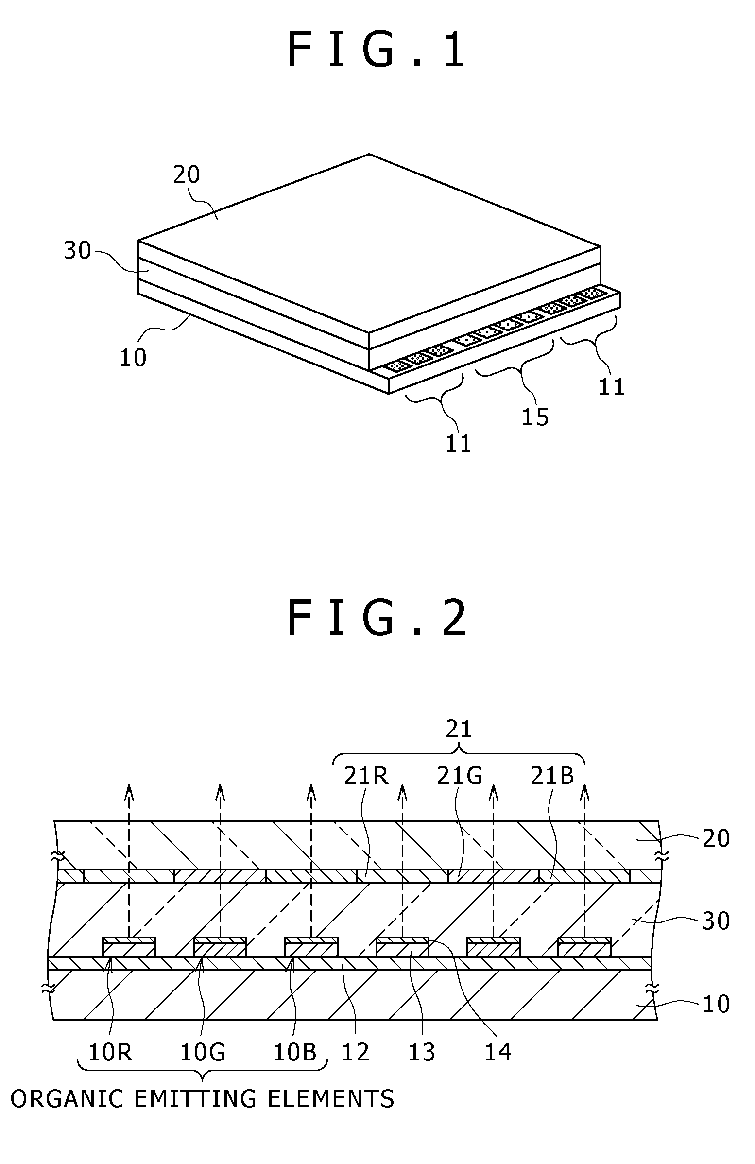
[0019]The display device constructed as outlined below is exemplified by an organic EL display device of top emission type in complete solid sealed structure.

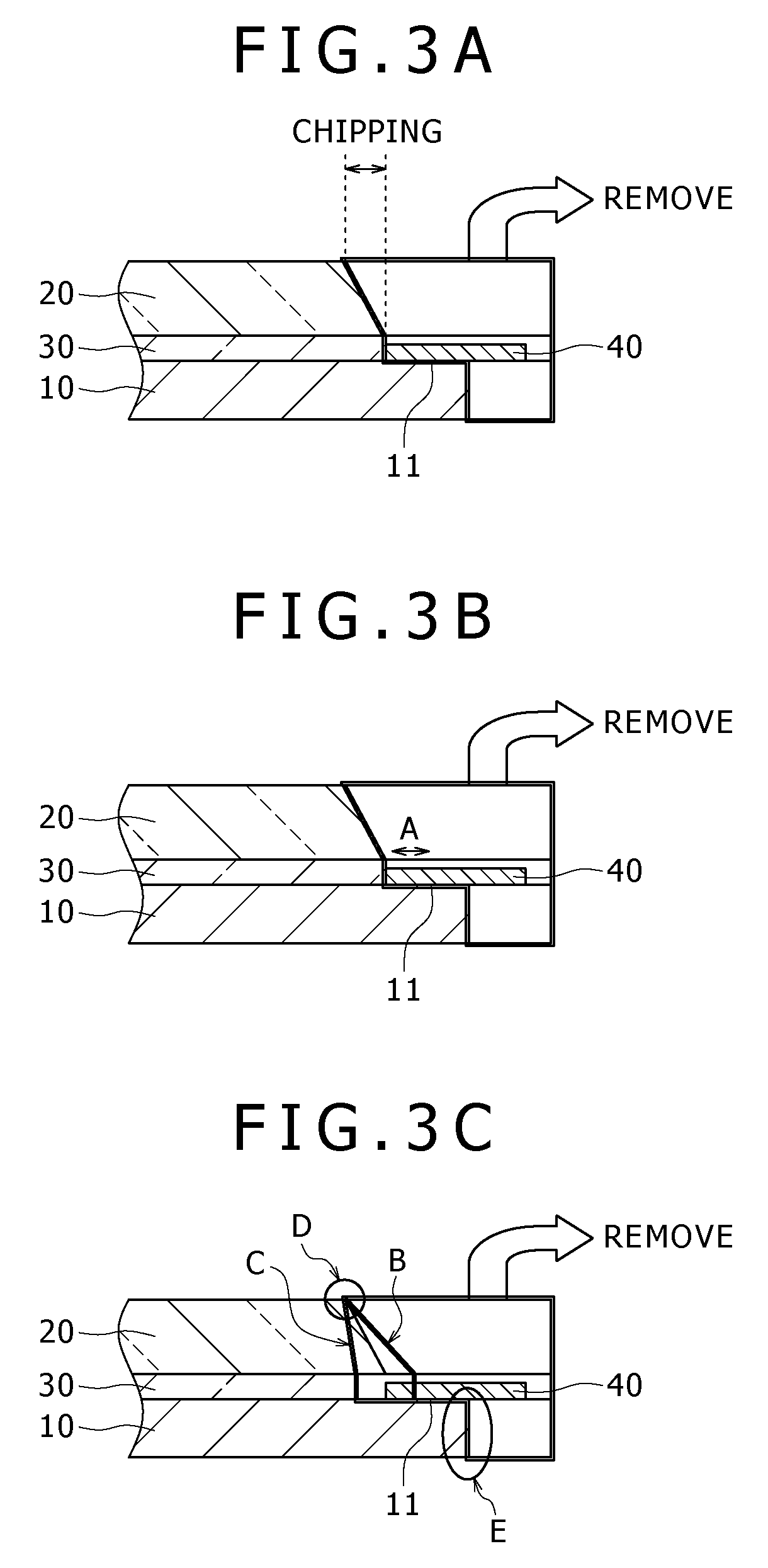
[0020]FIG. 1 is a schematic perspective view showing the structure of the organic EL display device. The illustrated organic EL display device is composed of an element substrate 10 and a sealing substrate 20, which face each other and adhere to each other over their entire surface by an adhesive layer 30 of thermosetting resin. The element substrate 10 has on its one side a terminal area 11 for external electrical connection through which the organic EL element (mentioned later) is supplied with signals and electric power. The terminal area 11 is formed from titanium (Ti) and aluminum (Al). It has an exposed surface which is not covered w...


PUM


Abstract

Disclosed herein is a method for producing a display device and a display device produced thereby. The method includes the steps of: forming on an element substrate terminal areas for electrical connection of display elements with external circuits; covering the terminal areas with a protective member; sealing the element substrate with a sealing substrate placed thereon, with an adhesive layer interposed between them in such a way as to cover the display elements on the element substrate and also cover the protective member; and removing part of the laminate body composed of the element substrate, the adhesive layer, and the sealing substrate and also removing the protective member, thereby exposing the terminal areas. The step of forming the terminal areas is carried out in such a way that the terminal areas are formed at two or more separate positions and pseudo terminal areas corresponding to the terminal areas are also formed between the separate positions.

Description

CROSS REFERENCES TO RELATED APPLICATIONS[0001]The present invention contains subject matter related Japanese Patent Application JP 2007-174688 filed in the Japan Patent Office on Jul. 3, 2007, the entire contents of which being incorporated herein by reference.BACKGROUND OF THE INVENTION[0002]1. Field of the Invention[0003]The present invention relates to a method for producing a display device and a display device, the display device having display elements such as organic light-emitting elements. More particularly, the present invention relates to a method for producing a display device and a display device, the display device being that of so-called complete solid sealed structure in which a driving panel having display elements is attached to a sealing panel with an adhesive layer interposed between them.[0004]2. Description of the Related Art[0005]It is recently expected that organic EL (electroluminescence) display devices having organic EL elements will replace liquid crystal...

Claims


Application Information

Patent Timeline
Patent Type & Authority Applications(United States)
IPC IPC(8): H01J9/20
CPCH01L27/3223H01L27/3276H01L27/3288H05B33/06H01L51/5281H05B33/04H01L51/5237H10K59/88H10K59/131H10K59/179H10K59/8791H10K59/871H10K50/841H10K50/86
Inventor MORIKAWA, SHINICHIROMINAMIKAWA, ATSUSHI
Owner SONY CORP
Features
  • Generate Ideas
  • Intellectual Property
  • Life Sciences
  • Materials
  • Tech Scout
  • Unparalleled Data Quality
  • Higher Quality Content
  • 60% Fewer Hallucinations
Learn More