Semiconductor device and semiconductor device fabrication method

a semiconductor device and semiconductor technology, applied in the field of semiconductor devices, can solve the problems of reduced reliability of wiring, increased resistance of wiring, and difficulty in miniaturizing semiconductor devices, and achieve the effect of superior reliability and superior reliability

Inactive Publication Date: 2009-01-15
SHINKO ELECTRIC IND CO LTD
View PDF8 Cites 16 Cited by
  • Summary
  • Abstract
  • Description
  • Claims
  • Application Information

AI Technical Summary

Benefits of technology

[0021]In the fabrication method, the semiconductor device can be fabricated which can be miniaturized and which has superior reliability.
[0022]According to the invention, there can ...

Problems solved by technology

Because of this, there has been caused a problem that the miniaturization of the semiconductor device becomes difficult.
In addition, in the semiconductor device, the routing of the wiring that is ...

Method used


Image

  • Semiconductor device and semiconductor device fabrication method
  • Semiconductor device and semiconductor device fabrication method
  • Semiconductor device and semiconductor device fabrication method

Examples


first embodiment

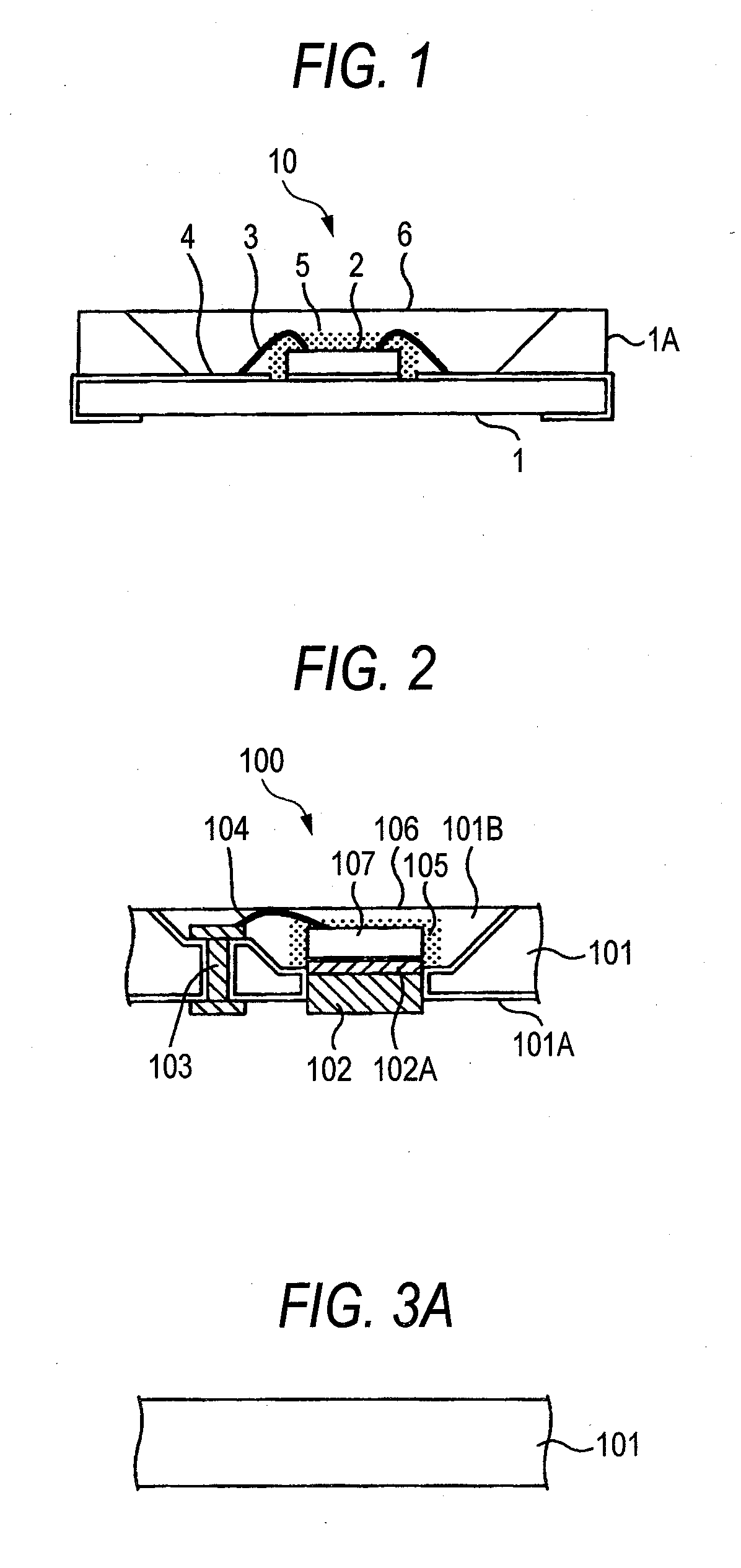
[0051]FIG. 2 is a sectional view which shows exemplarily a semiconductor device 100 according to a first embodiment of the invention. Referring to FIG. 2, in the semiconductor device 100 according to this embodiment, a light emitting element 107 which is made up of, for example, an LED is mounted on a substrate 101 which is made of, for example, a silicon. A resin 105 containing a fluorescent material is coated on the light emitting element 107. The color of light emitted from the light emitting element and the color light emitted from of the fluorescent material can be mixed for use by so coating the resin 105, thereby making it possible to control the color of light emitted from the semiconductor device in various ways. In addition, for example, a silicon based or epoxy based resin layer 106 is formed in such a manner as to cover the resin 105 for protection of the resin 105. Additionally, the fluorescent material may be mixed into the whole of the resin layer 106.

[0052]A recessed...

second embodiment

[0073]FIG. 4 is a drawing which exemplarily shows a semiconductor device 100A according to a second embodiment of the invention. In the drawing, however, like reference numerals will be given to like portions to those which have already been described above so as to omit the repetition of similar descriptions. In addition, portions about which no particular description will be made have the similar constructions to those of the semiconductor device 100 described in the first embodiment and provide the same advantages provided thereby.

[0074]Referring to FIG. 4, in a semiconductor device 100A according to this embodiment, two bonding wires 104 and two through electrodes 103 to which the two bonding wires 104 are connected are formed. In this way, the number of such constructions in which the bonding wire and the through electrode to which the bonding wire is connected are combined may be increased as required. As this occurs, the number of wiring systems which are provided to be conne...

third embodiment

[0075]FIG. 5 is a drawing which exemplarily shows a semiconductor device 100B according to a third embodiment of the invention. In the drawing, however, like reference numerals will be given to like portions to those which have already been described above so as to omit the repetition of similar descriptions. In addition, portions about which no particular description will be made have the similar constructions to those of the semiconductor device 100 described in the first embodiment and provide the same advantages provided thereby.

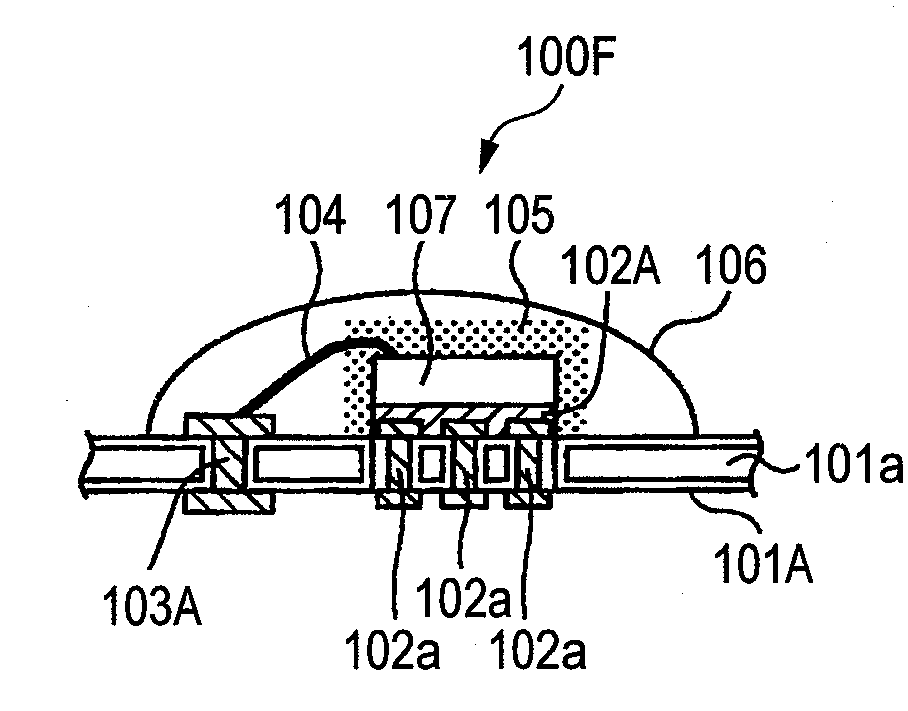
[0076]Referring to FIG. 5, in a semiconductor device 100B according to this embodiment, three through electrodes 102a, which each corresponds to the through electrode 102 of the semiconductor device 100, are formed. In this way, the through electrode which is connected with the light emitting element 107 may be provided two or more.


PUM


Abstract

There is provided a semiconductor device in which a light emitting element is mounted on a substrate, having a bonding wire which is connected to the light emitting element, and a through electrode which is connected to the bonding wire and is formed in such a manner as to pass through the substrate at a position lying directly below a connecting portion with the bonding wire.

Description

[0001]This application claims priority to Japanese Patent Application No. 2006-115725, filed Apr. 19, 2006, in the Japanese Patent Office. The priority application is incorporated by reference in its entirety.TECHNICAL FIELD[0002]The present disclosure relates to a semiconductor device in which a light emitting element is mounted on a substrate and a fabrication method of the semiconductor device.RELATED ART[0003]Semiconductor devices of various shapes have been proposed for semiconductor devices in which a light emitting element such as an LED is mounted on a substrate. For example, FIG. 1 is a drawing which exemplarily shows one of those semiconductor devices which have been proposed in the related-art.[0004]Referring to FIG. 1, in a semiconductor device 10, a light emitting element 2 made up of an LED coated with a fluorescent material 5 is mounted on a substrate made of, for example, a ceramic. In addition, a wall portion 1A is formed on the substrate 1 in such a manner as to su...

Claims


Application Information

Patent Timeline
IPC IPC(8): H01L33/00H01L21/00H01L33/50H01L33/54H01L33/56H01L33/60H01L33/62H01L33/64
CPCH01L24/97H01L2924/12041H01L33/62H01L33/64H01L33/647H01L2224/48091H01L2224/48227H01L2224/73265H01L2224/97H01L2924/01029H01L2924/01033H01L2924/01047H01L2924/01078H01L2924/01079H01L33/486H01L2224/32245H01L2924/10253H01L2924/01019H01L2924/01006H01L2224/32225H01L2224/85H01L2924/00014H01L2924/00H01L2924/00012H01L2224/92247H01L24/73H01L2924/15787
Inventor HIGASHI, MITSUTOSHIMURAYAMA, KEISHIRAISHI, AKINORITAGUCHI, YUICHI
Owner SHINKO ELECTRIC IND CO LTD
Why Eureka
Try Eureka