Motherboard

a technology for motherboards and motherboards, applied in the direction of printed circuit stress/warp reduction, electrical apparatus construction details, electrical apparatus casings/cabinets/drawers, etc., can solve the problems of easy damage to the tin balls located at these corners, affecting the performance of the motherboard, etc., and achieve the effect of effectively minimizing or preventing the damage to the chips

Inactive Publication Date: 2009-01-15
HON HAI PRECISION IND CO LTD
View PDF6 Cites 5 Cited by
  • Summary
  • Abstract
  • Description
  • Claims
  • Application Information

AI Technical Summary

Benefits of technology

[0008]A motherboard includes a printed circuit board, a first chip and a second chip arranged on the printed circuit board in parallel. A plurality of securing holes are defined in the printed circuit board around the first chip. At least one isolating hole is defined in the printed circuit board between the second chip and a first line determined by two of the securing holes close to the second chip. Should the printed circuit board suffer from an impact, damage to the chips may be effectively minimized or prevented.

Problems solved by technology

However, due to the dangers of leaded tin balls polluting the environment and damaging health of people, nonleaded tin balls are now commonly used in the process of mounting a semiconductor chip to a printed circuit board.
However, because of the poor capability of non-leaded tin balls to resist shock, they are easily damaged when the printed circuit board suffers an impact, thereby affecting performance of chips on the motherboard.
Therefore, the tin balls located at these corners are easily damaged by impact to the PCB 10′.

Method used


Image

  • Motherboard
  • Motherboard
  • Motherboard

Examples


Embodiment Construction

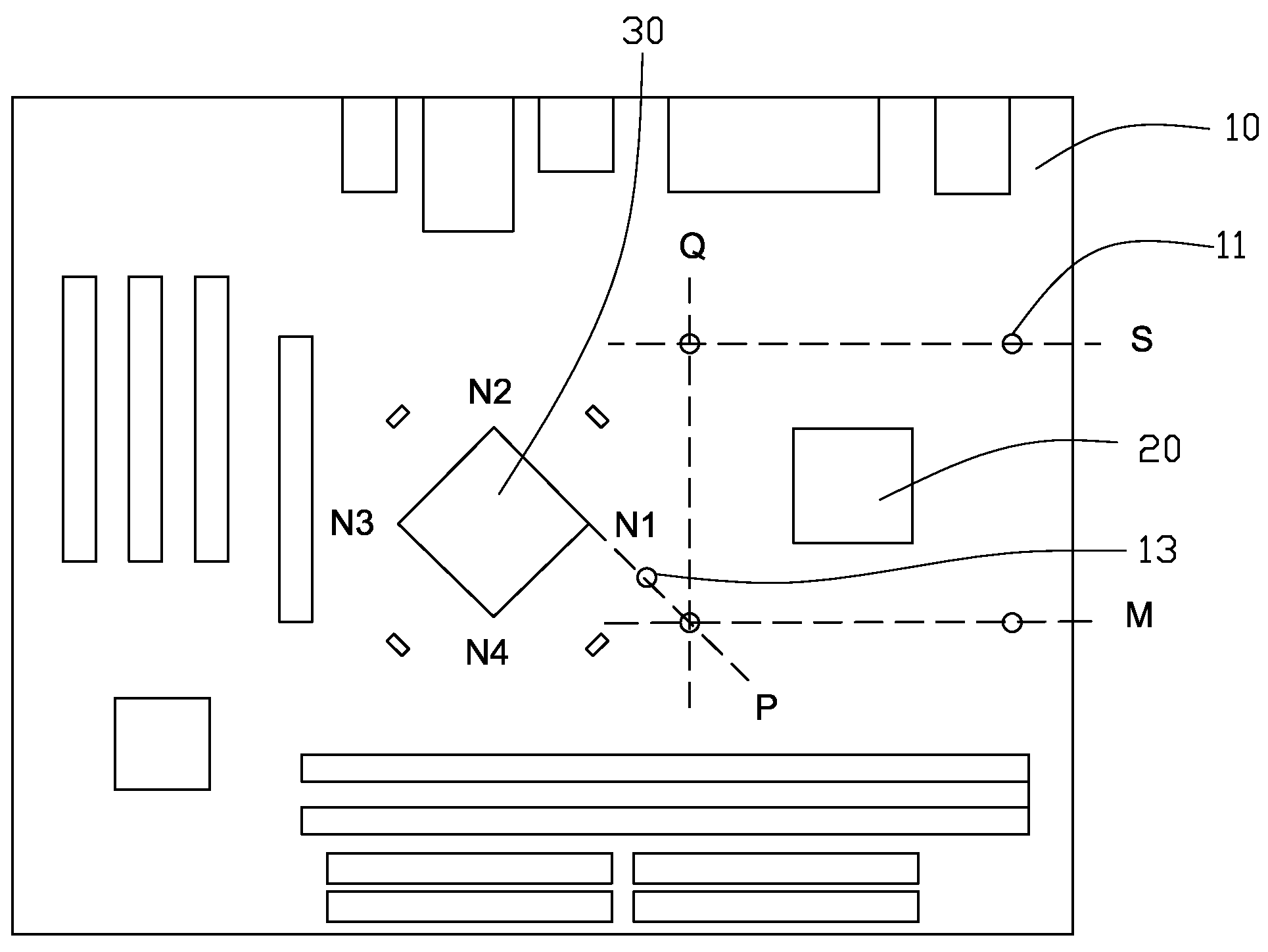
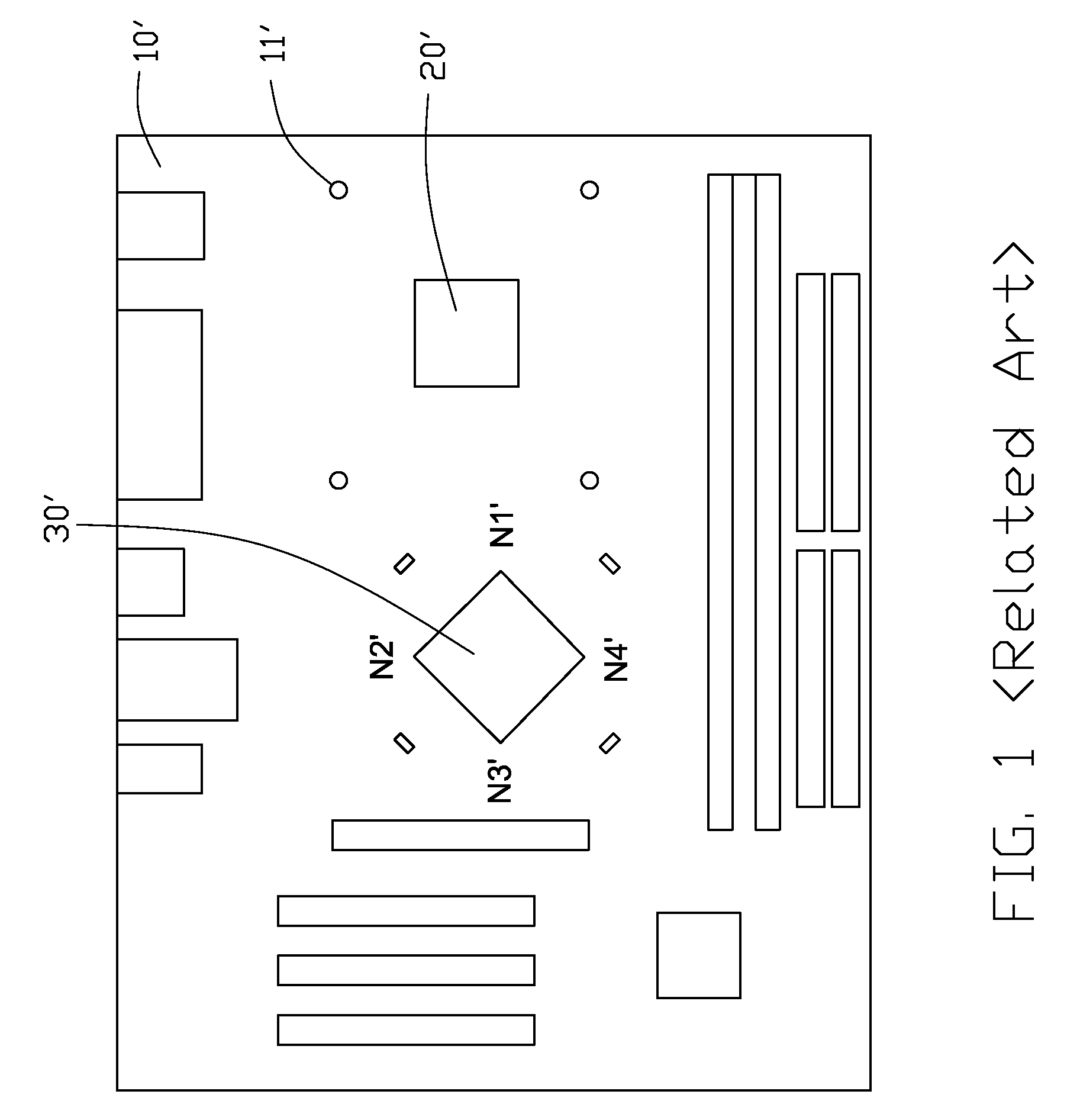
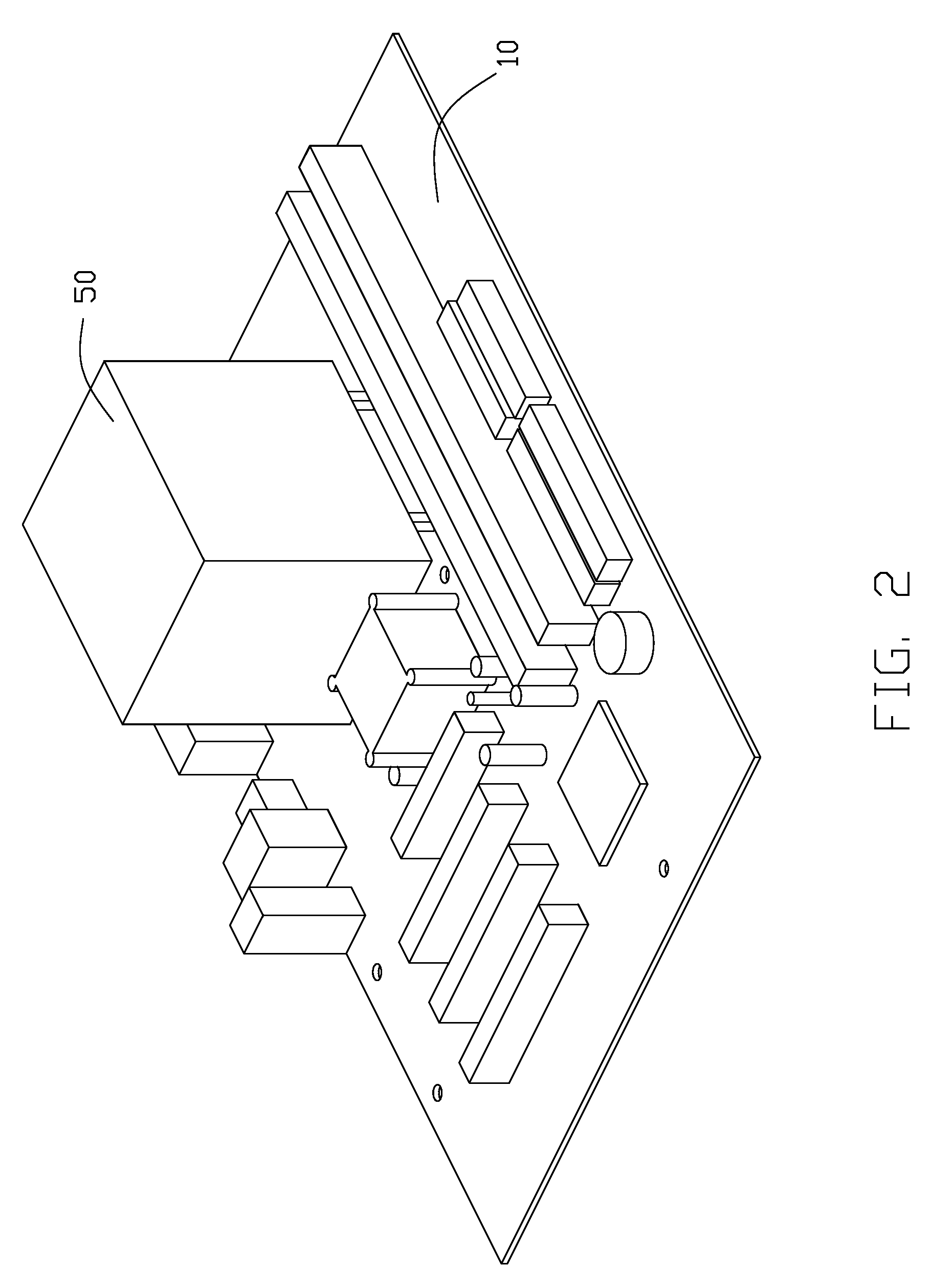
[0014]Referring to FIGS. 2 and 3, a motherboard according to a first embodiment of the present invention includes a printed circuit board (PCB) 10, a first chip, such as a central processing unit (CPU) 20, and a second chip, such as a north bridge chip 30, arranged on the PCB 10 in parallel. The CPU 20 and north bridge chip 30 are respectively jointed to the PCB 10 via a plurality of tin balls. Four securing holes 11 are defined in the PCB 10 around the CPU 20, for securing a heat dissipating module 50 on the CPU 20. A line S determined by two adjacent securing holes 11 is parallel to a line M determined by the other two adjacent securing holes 11. The CPU 20 is square or rectangular, and centrally located in a square or rectangular area determined by the four securing holes 11. The north bridge chip 30 is also square or rectangular, including four corners N1, N2, N3, and N4. A line determined by two opposite corners N1 and N3 of the north chip 30 is located between the parallel lin...


PUM


Abstract

A motherboard includes a printed circuit board, a first chip and a second chip arranged on the printed circuit board in parallel. A plurality of securing holes are defined in the printed circuit board around the first chip. At least one isolating hole is defined in the printed circuit board between the second chip and a first line determined by two of the securing holes close to the second chip. Should the printed circuit board suffer an impact, damage to the chips may be effectively minimized or prevented.

Description

BACKGROUND[0001]1. Field of the Invention[0002]The present invention relates to motherboards for computers, particularly to a motherboard configured to prevent or minimize damage to a semiconductor chip on the motherboard when the motherboard suffers an impact.[0003]2. Description of Related Art[0004]In the design process of a motherboard, stability of chips on the motherboard is a prime concern. In manufacturing of a motherboard, semiconductor chips are usually mounted on a printed circuit board via tin balls. A conventional tin ball is made with lead. Because of good capability of lead for resisting shock, the tin ball is not easily damaged. However, due to the dangers of leaded tin balls polluting the environment and damaging health of people, nonleaded tin balls are now commonly used in the process of mounting a semiconductor chip to a printed circuit board. However, because of the poor capability of non-leaded tin balls to resist shock, they are easily damaged when the printed ...

Claims


Application Information

Patent Timeline
Patent Type & Authority Applications(United States)
IPC IPC(8): H05K7/20H05K7/02
CPCH05K1/0203H05K2201/10734H05K2201/09063H05K1/0271
Inventor CHAO, CHIH-HANGLIN, YU-HSUWU, JENG-DA
Owner HON HAI PRECISION IND CO LTD
Why Eureka
Try Eureka