CMOS Image Sensor and Method for Manufacturing the Same

a metal oxide semiconductor and image sensor technology, applied in the direction of diodes, semiconductor devices, radiation control devices, etc., can solve the problems of high power consumption, complicated manufacturing process of ccd, complicated drive mode, etc., and achieve the effect of minimizing or preventing damage to the semiconductor substra

Inactive Publication Date: 2007-06-28
DONGBU HITEK CO LTD
View PDF2 Cites 4 Cited by
  • Summary
  • Abstract
  • Description
  • Claims
  • Application Information

AI Technical Summary

Benefits of technology

[0039] Accordingly, an object of embodiments of the present invention is to provide a CMOS image sensor and a method of fabricating the same, capable of minimizing or preventing damage from occurring in the semiconductor substrate when forming a gate electrode and an insulating layer sidewall.

Problems solved by technology

However, the CCD has various disadvantages, such as a complicated drive mode and high power consumption.
Also, the CCD requires multi-step photo processes, so the manufacturing process for the CCD is complicated.
In addition, since it is difficult to integrate a controller, a signal processor, and an analog / digital converter (A / D converter) onto a single chip of the CCD, the CCD is not suitable for compact-size products.
However, the conventional method of fabricating the CMOS image sensor has following problems.
When the gate is formed by the conventional CMOS fabrication process, damage is caused to the surface of the photodiode during the etching process for patterning the gate, thereby incurring dark current of the photodiode.
That is, when forming the gate electrode and the insulating layer sidewall, damage occurs on the surface of the semiconductor substrate.
In addition, since the insulating layer sidewall is made from a silicon nitride layer, the surface of the semiconductor substrate is subject to stress due to silicon nitride, so that leakage current is generated, degrading the performance of the image sensor.

Method used


Image

  • CMOS Image Sensor and Method for Manufacturing the Same
  • CMOS Image Sensor and Method for Manufacturing the Same
  • CMOS Image Sensor and Method for Manufacturing the Same

Examples


Embodiment Construction

[0047] Hereinafter, a CMOS image sensor and a method of fabricating the same according to the preferred embodiments of present invention will be described with reference to the accompanying drawings.

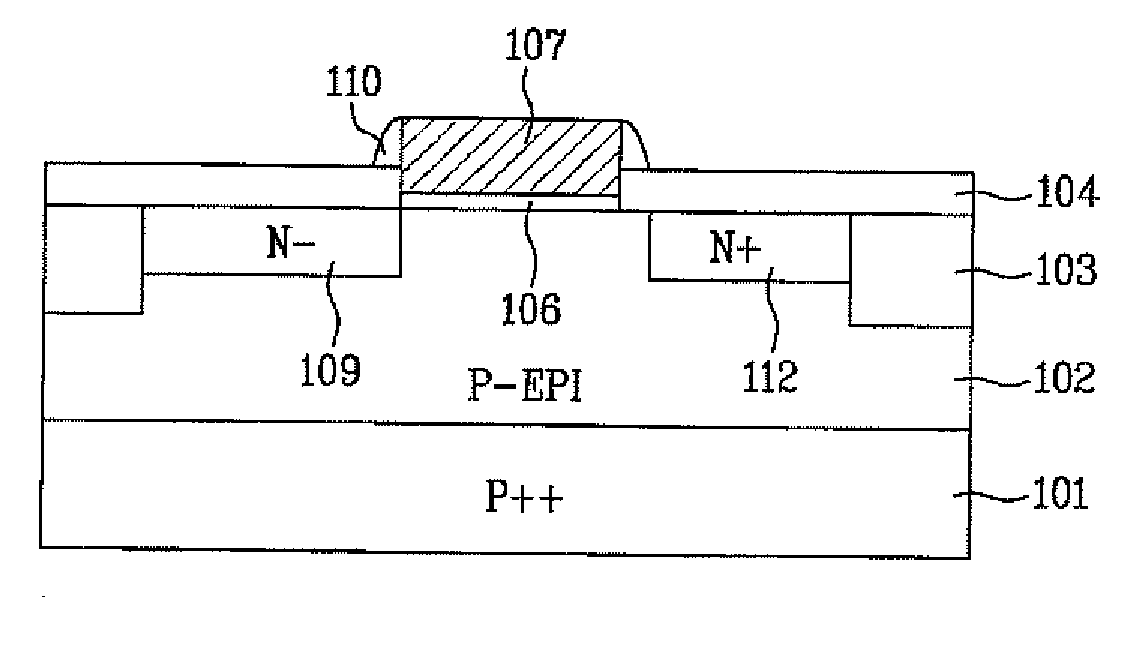
[0048]FIG. 4 is a sectional view illustrating the structure of a CMOS image sensor according to an embodiment of the present invention.

[0049] As shown in FIG. 4, the CMOS image sensor can include a p− type epitaxial layer 102 formed on a p++ type conductive semiconductor substrate 101, on which a photodiode area and a transistor area are defined; an isolation layer 103 formed on a field area to define an active area of the semiconductor substrate 101; a gate electrode 107 formed on the active area of the semiconductor substrate 101 with a gate insulating layer 106 interposed therebetween; a low-density n− type diffusion area 109 formed in the photodiode area at one side of the gate electrode 107; a high-density n+ type diffusion area 112 formed in the transistor area at the other side ...


PUM


Abstract

A CMOS image sensor and method for fabricating same are provided. The CMOS image sensor can include a gate electrode formed on an active area of a first conductive type semiconductor substrate, on which a photodiode area and a transistor area are defined; a low-density second conductive type diffusion region formed on the photodiode area at a first side of the gate electrode; a high-density second conductive the diffusion region formed on the transistor area at a second side of the gate electrode; an insulating layer formed on the semiconductor substrate at both sides of the gate electrode with a thickness less than a thickness of the gate electrode, but greater than a thickness of a gate insulating layer; and insulating layer sidewalls formed on the insulating layer at both sides of the gate electrode.

Description

RELATED APPLICATION(S) [0001] This application claims priority under 35 U.S.C. §119(e) of Korean Patent Application No. 10-2005-0132727 filed Dec. 28, 2005, which is incorporated herein by reference in its entirety. FIELD OF THE INVENTION [0002] The present invention relates to a complementary metal oxide semiconductor (CMOS) image sensor. BACKGROUND OF THE INVENTION [0003] In general, an image sensor is a semiconductor device for converting optical images into electric signals, and is mainly classified as a charge coupled device (CCD) or a CMOS image sensor. [0004] The CCD has a plurality of photodiodes (PDs), which are arranged in the form of a matrix in order to convert optical signals into electric signals. The CCD includes a plurality of vertical charge coupled devices (VCCDs) provided between photodiodes and vertically arranged in the matrix so as to transmit electrical charges in the vertical direction when the electrical charges are generated from each photodiode. The CCD al...

Claims


Application Information

Patent Timeline
Patent Type & Authority Applications(United States)
IPC IPC(8): H01L31/06
CPCH01L27/14603H01L27/14609H01L27/1462H01L27/14643H01L27/14689H01L27/146
Inventor LIM, KEUN HYUK
Owner DONGBU HITEK CO LTD
Why Eureka
Try Eureka