Analog to digital converter with a series of delay units
- Summary
- Abstract
- Description
- Claims
- Application Information
AI Technical Summary
Benefits of technology
Problems solved by technology
Method used
Image

Examples
embodiment 1
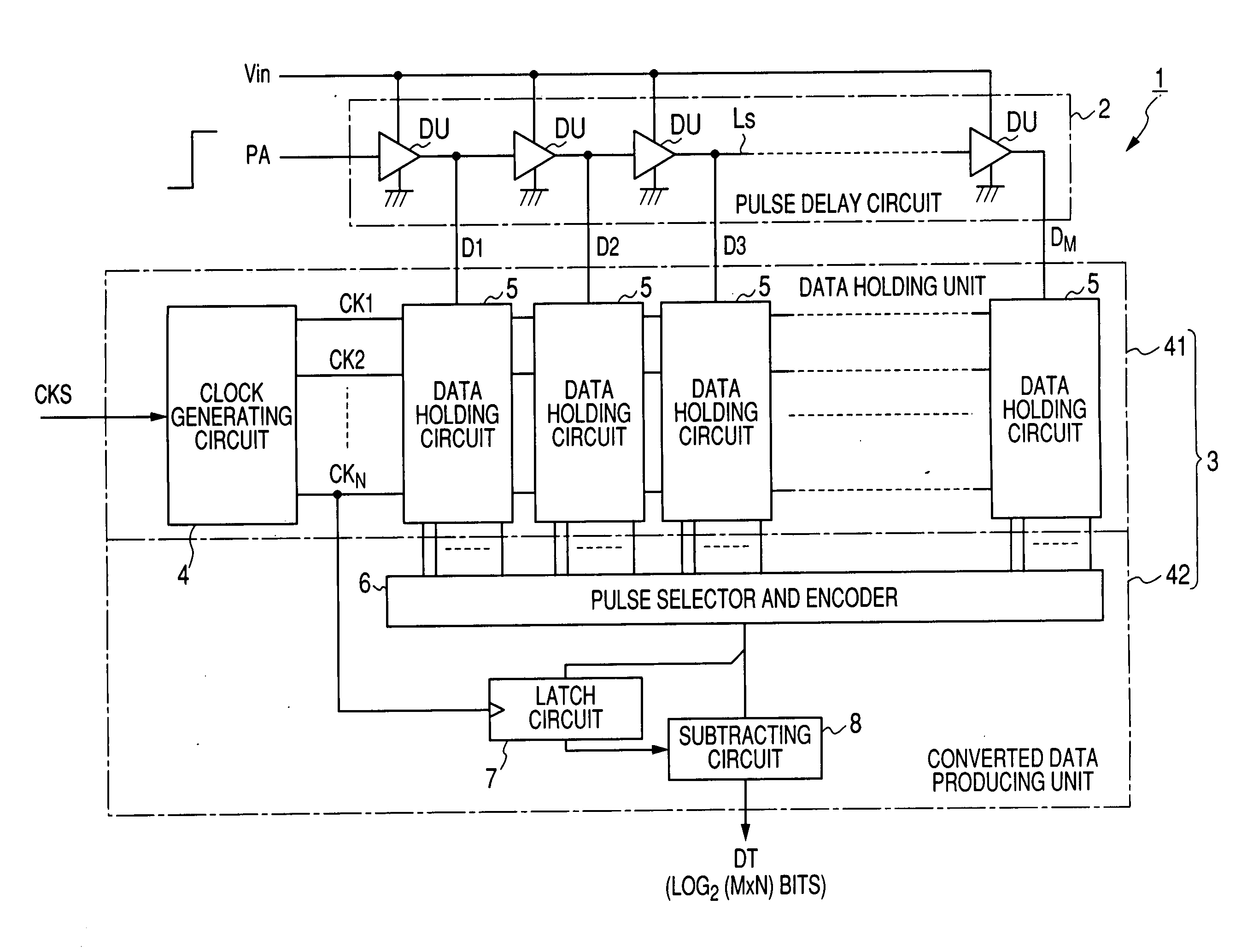
[0063]FIG. 4 is a block diagram of an A / D converter according to the first embodiment. As shown in FIG. 4, a TDA type analog-to-digital (A / D) converter 1 has a pulse delay circuit 2 and a coding circuit 3. The delay circuit 2 has a plurality of delay units DU arranged in M stages (M is an integer equal to or higher than 2). Preferably, the value M equals the s-th power of 2 (M=2s; s is an integer). Each delay unit DU is formed of a series of gate circuits such as even-numbered inverters. The delay units DU simultaneously receive an analog input signal (i.e., voltage signal) Vin as a driving voltage and have the same delay time Td corresponding to a voltage level of the signal Vin. As the level of the signal Vin is heightened, the delay time Td is shortened. A pulse signal PA passes through a signal transmission line Ls on which the delay units DU are serially arranged, so that the pulse PA is delayed in each of the delay units DU serially arranged. Outputs D1 to DM of the delay unit...
embodiment 2
[0110]FIG. 12 is a block diagram of an A / D converter according to the second embodiment.
[0111]As shown in FIG. 12, a TAD type A / D converter 10 has the pulse delay circuit 2 and a coding circuit 30 for producing A / D converted data DT indicating a quantity of movement of the pulse signal PA. The coding circuit 30 has a data holding unit 43 and the producing unit 42. The holding unit 43 has M data holding circuits 50 corresponding to the respective delay units DU to latch the outputs Di of the circuit 2 and to hold M×N pieces of latched data.
[0112]FIG. 13 is a view showing the structure of each holding circuit 50 of the converter 10.
[0113]As shown in FIG. 13, each holding circuit 50 has N delay elements DL1 to DLN and the N flip-flop circuits (i.e., latch circuits) Fi1 to FiN corresponding to the respective delay elements DL1 to DLN. Each delay element DLj (j=1, 2, - - - , N) delays the output Di of the corresponding delay unit DU by a multiplied unit time ΔTnj (ΔTnj=j×ΔT) equal to j t...
embodiment 3
[0118]There is a case where bit error occurs in the latched data supplied from the holding circuits 5. In this case, the combined data Q composed of the latched data undesirably has a plurality of bit boundaries. Further, bit error sometimes occurs in a series of bits of the combined data Q. In this embodiment, even when bit error occurs in the latched data such that the combined data Q has a plurality of bit boundaries, the latched data are appropriately corrected to form a piece of corrected data Qc having only one bit boundary.
[0119]FIG. 14 is a block diagram of an A / D converter according to the third embodiment.
[0120]As shown in FIG. 14, a TAD type A / D converter 11 has the pulse delay circuit 2 and a coding circuit 31 for producing A / D converted data DT indicating a quantity of movement of the pulse signal PA. The coding circuit 31 has the data holding unit 41 and a converted data producing unit 44. The producing unit 44 has a combined data correcting circuit 9 for receiving the...
PUM
 Abstract
Description
Claims
Application Information
 - R&D
- Intellectual Property
- Life Sciences
- Materials
- Tech Scout
- Unparalleled Data Quality
- Higher Quality Content
- 60% Fewer Hallucinations
Browse by: Latest US Patents, China's latest patents, Technical Efficacy Thesaurus, Application Domain, Technology Topic, Popular Technical Reports.
© 2025 PatSnap. All rights reserved.Legal|Privacy policy|Modern Slavery Act Transparency Statement|Sitemap|About US| Contact US: help@patsnap.com