Booster circuit and non-volatile memory including the same

Active Publication Date: 2018-05-24
ABLIC INC
View PDF1 Cites 0 Cited by
  • Summary
  • Abstract
  • Description
  • Claims
  • Application Information

AI Technical Summary

Benefits of technology

[0015]With the booster circuit according to the present invention, a time period in which voltage stress is applied to each of the booster cells in the last stage can be shortened by providing the

Problems solved by technology

However, optimal design of the charge transfer transistors in the respective booster cells in accordance with the potentials

Method used


Image

  • Booster circuit and non-volatile memory including the same
  • Booster circuit and non-volatile memory including the same
  • Booster circuit and non-volatile memory including the same

Examples


Example

[0019]Now, an embodiment of the present invention is described with reference to the drawings.

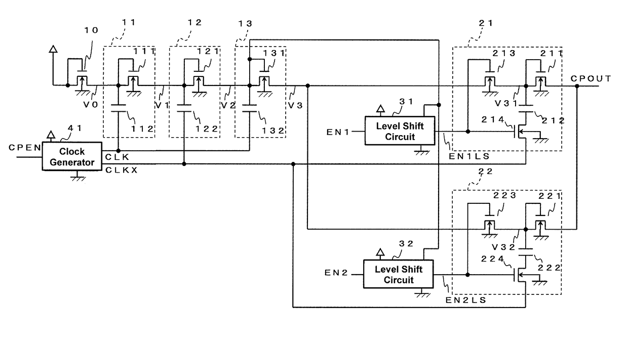
[0020]FIG. 1 is a circuit diagram of a booster circuit according to the embodiment of the present invention. The following description is made of a case in which the number of boost stages of the booster circuit is 4 (N=4).

[0021]The booster circuit according to this embodiment includes a diode-connected NMOS transistor 10, booster cells 11 to 13, booster cells 21 and 22, level shift circuits 31 and 32, and a clock generator 41.

[0022]The booster cells 11 to 13 each include three terminals, namely, an input terminal, an output terminal, and a clock input terminal, and include charge transfer transistors 111, 121, and 131 formed of diode-connected NMOS transistors, and boost capacitors 112, 122, and 132, respectively. Each of the charge transfer transistors 111, 121, and 131 has a gate connected to the input terminal of a corresponding one of the booster cells 11 to 13, a source connected to o...


PUM


Abstract

To obtain a booster circuit capable of reducing voltage stress applied to a booster cell, provided is a booster circuit including a plurality of booster cells connected in series. Each of the plurality of booster cells includes a charge transfer transistor connected between an input terminal and an output terminal, and a boost capacitor connected between the input terminal and a clock terminal. Among the plurality of booster cells, a plurality of booster cells at least in a last stage are connected in parallel so that the plurality of booster cells connected in parallel are connected to a booster cell in a previous stage of the last stage by switching the plurality of booster cells in the last stage in accordance with a boosting operation.

Description

RELATED APPLICATIONS[0001]This application claims priority under 35 U.S.C. § 119 to Japanese Patent Application No. 2016-226978 filed on Nov. 22, 2016, the entire content of which is hereby incorporated by reference.BACKGROUND OF THE INVENTION1. Field of the Invention[0002]The present invention relates to a booster circuit including a charge transfer transistor and a boost capacitor, and to a non-volatile memory including the booster circuit.2. Description of the Related Art[0003]An EEPROM which is a non-volatile memory requires a high voltage to rewrite data in a memory cell, and hence includes a booster circuit.[0004]FIG. 3 is a circuit diagram for illustrating a related-art booster circuit.[0005]In the related-art booster circuit, there is adopted a loop connection in which booster cells 51 to 54 are connected in series and output of the booster cell 54 and input of the booster cell 51 are connected to each other. The booster cells 51 to 54 are configured to receive input of cloc...

Claims


Application Information

Patent Timeline
IPC IPC(8): G11C5/14G11C16/14H02M3/07G11C16/30
CPCG11C5/145G11C16/14H02M3/07G11C16/30H02M2003/078H02M3/073H02M3/075H02M3/078
Inventor MITANI, MAKOTO
Owner ABLIC INC
Why Eureka
Try Eureka