Surface emitting apparatus and image display apparatus using the surface emitting apparatus

a surface emitting apparatus and surface technology, applied in lighting and heating apparatus, planar/plate-like light guides, instruments, etc., can solve the problems of difficult to produce output light with high luminance uniformity, large cost, etc., and achieve the effect of improving luminance uniformity and small apparatus siz

Inactive Publication Date: 2009-01-22
PANASONIC CORP
View PDF3 Cites 3 Cited by
  • Summary
  • Abstract
  • Description
  • Claims
  • Application Information

AI Technical Summary

Benefits of technology

[0009]It is therefore an object of the present invention to provide a surface emitting apparatus and image display apparatus using this surface emitting apparatus that enables improved luminance uniformity and smaller apparatus sizes.

Problems solved by technology

Further, the planar light source disclosed in Japanese Patent Application Laid-Open No. 2002-169480 uses a reflection volume hologram, which results in a greater cost and makes it difficult to produce output light with high luminance uniformity.

Method used


Image

  • Surface emitting apparatus and image display apparatus using the surface emitting apparatus
  • Surface emitting apparatus and image display apparatus using the surface emitting apparatus
  • Surface emitting apparatus and image display apparatus using the surface emitting apparatus

Examples


embodiment 1

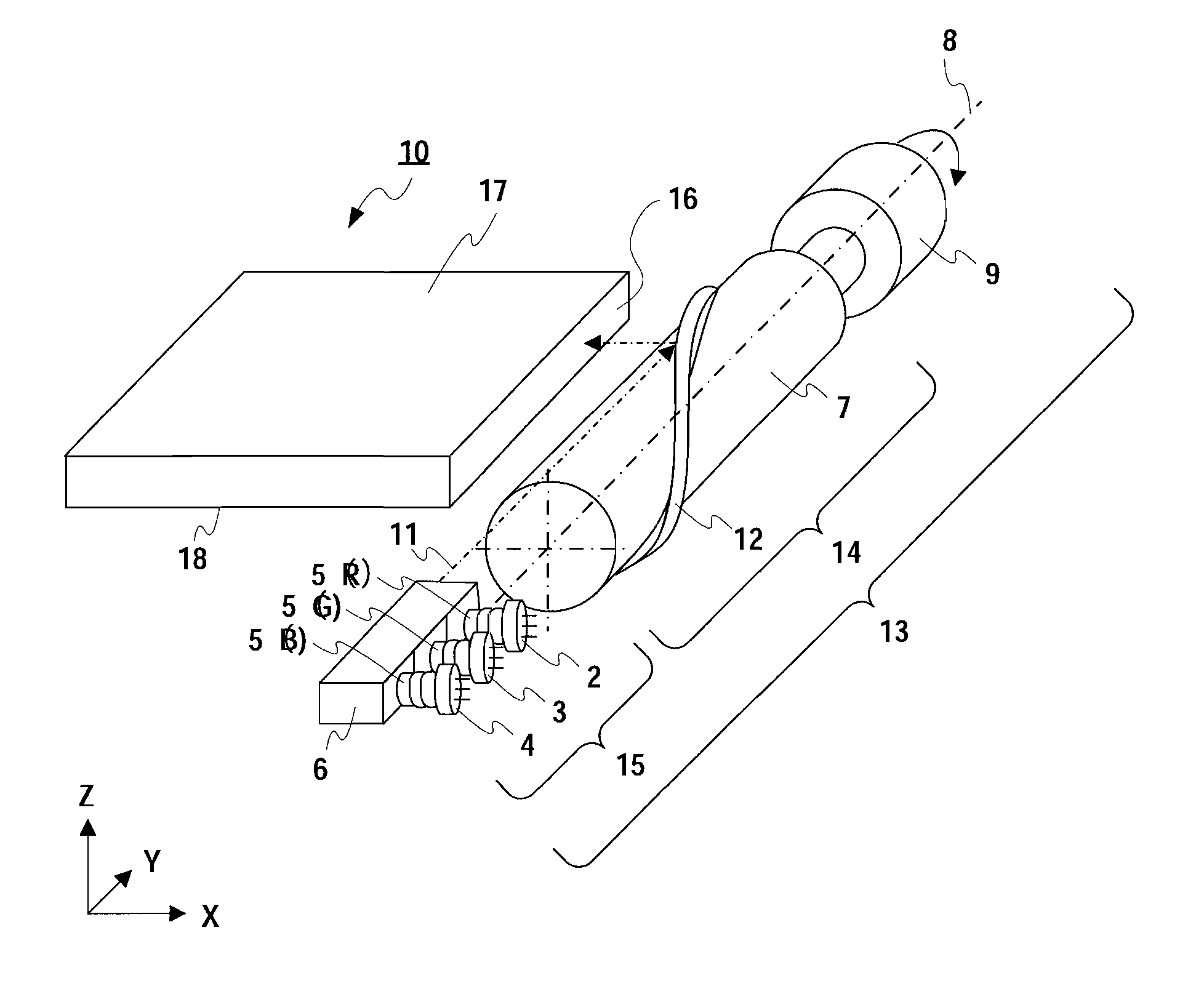
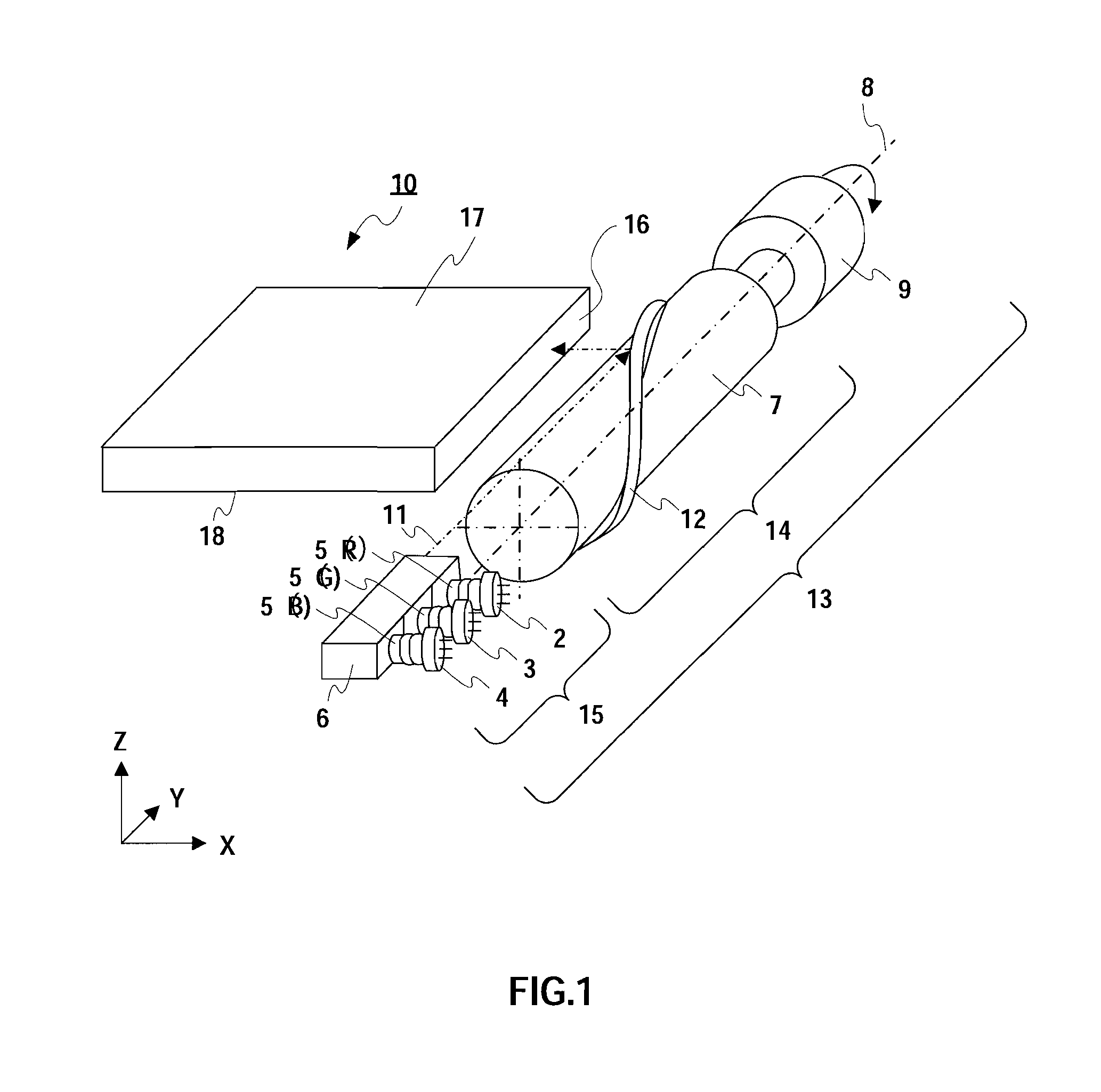
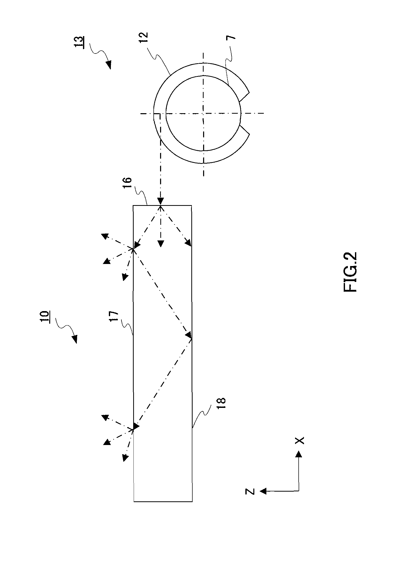
[0053]FIG. 1 is a schematic perspective view of a surface emitting apparatus according to Embodiment 1 of the present invention. FIG. 2 is a schematic cross sectional view of the surface emitting apparatus of FIG. 1. The surface emitting apparatus has light guide plate 10 and light scanning mechanism 13. Further, in the following embodiments, the longitudinal direction of inlet end face 16 will be referred to as “Y-axis” direction and two axes that cross with each other and with the Y-axis at right angles will be referred to as “X-axis” and “Z-axis.” The Z-axis is oriented to the lateral direction (i.e. thickness direction) of inlet end face 16 and the X-axis is oriented to the direction away from inlet end face 16.

[0054]Light scanning mechanism 13 has light source section 15, helical mirror 14 and motor 9 that rotates helical mirror 14. Light source section 15 has red conductor laser 2 that produces a light of a 635 nm wavelength, green SHG laser 3 that produces a light of a 540 nm...

embodiment 2

[0066]Next, the surface emitting apparatus according to Embodiment 2 of the present invention will be described. FIG. 4A is a schematic perspective view of the surface emitting apparatus according to Embodiment 2 of the present invention. FIG. 4B is a schematic cross sectional view of the surface emitting apparatus of FIG. 4A. Although the surface emitting apparatus according to the present embodiment has virtually the same configuration as the surface emitting apparatus according to Embodiment 1 except for the arrangement of the helical mirror. In the following embodiments, differences from Embodiment 1 will be mainly described, and the same components as in Embodiment 1 will be assigned the same reference numerals and repetition of description will be omitted.

[0067]With Embodiment 1, helical mirror 14 and light guide plate 10 are arranged such that the position of the part in reflector element 12 in the Z-axis direction where light is incident and the position of the middle of inl...

embodiment 3

[0070]Next, the surface emitting apparatus according to Embodiment 3 of the present invention will be described. FIG. 5A is a schematic top view of the surface emitting apparatus according to Embodiment 3 of the present invention. FIG. 5B is a schematic exploded view of helical mirror 14 shown in FIG. 5A. The surface emitting apparatus according to the present embodiment has virtually the same configuration as the surface emitting apparatus according to Embodiment 1 but is different from Embodiment 1 in arranging helical mirror 14 diagonally to light guide plate 10.

[0071]With Embodiment 1, helical mirror 14 and light guide plate 10 are arranged such that rotation axis 8 and inlet end face 16 of light guide plate 10 are parallel. However, with the present embodiment, helical mirror 14 is arranged such that rotation axis 8 is diagonal to inlet end face 16 of the light guide plate.

[0072]Similar to Embodiment 1, reflector element 12 is formed in helix on the outer peripheral surface of ...


PUM


Abstract

A surface emitting apparatus and image display apparatus using this surface emitting apparatus that enables improved luminance uniformity and smaller apparatus sizes. The surface emitting apparatus has a light source section that emits light, a light guide plate that guides light incident from an inlet face such that the light is emitted from a surface of an outlet face and a scanning section that scans the light emitted from the light source section on the inlet face of the light guide plate. The image display apparatus has the surface emitting apparatus and a display panel that is arranged on a side of the outlet face of the light guide plate.

Description

CROSS REFERENCE TO RELATED APPLICATIONS[0001]The disclosures of Japanese Patent Application No. 2008-138525, filed on May 27, 2008, Japanese Patent Application No. 2007-188507, filed on Jul. 19, 2007, Japanese Patent Application No. 2007-188508, filed on Jul. 19, 2007, Japanese Patent Application No. 2007-188509, filed on Jul. 19, 2007, Japanese Patent Application No. 2007-189704, filed on Jul. 20, 2007, and Japanese Patent Application No. 2007-190604 filed on Jul. 23, 2007, including the specifications, drawings and abstracts, are incorporated herein by reference in their entirety.BACKGROUND OF THE INVENTION[0002]1. Field of the Invention[0003]The present invention relates to a surface emitting apparatus and an image display apparatus using this surface emitting apparatus.[0004]2. Description of the Related Art[0005]Recently, accompanying the spread of mobile telephones and information devices, there are demands for thinner, high quality, and high efficiency image display apparatus...

Claims


Application Information

Patent Timeline
Patent Type & Authority Applications(United States)
IPC IPC(8): F21V8/00
CPCG02B6/002G02B6/0025H04M1/22G02B6/0031G02B6/0068G02B6/0028
Inventor YOSHIKAWA, MOTONOBUYAMAGUCHI, HIROSHIISHIMARU, KAZUHIKOYABUSHITA, ERINA
Owner PANASONIC CORP
Why Eureka
Try Eureka