Metallic pattern forming method, metallic pattern obtained thereby, printed wiring board using the same, and TFT wiring board using the same
a technology of metallic pattern and forming method, which is applied in the direction of superimposed coating process, resistive material coating, liquid/solution decomposition chemical coating, etc., can solve the problems of high frequency characteristics deterioration, expensive apparatus such as a -ray generating apparatus and an electron beam generating apparatus, and achieves excellent flatness, high frequency characteristics, and good resistance.
- Summary
- Abstract
- Description
- Claims
- Application Information
AI Technical Summary
Benefits of technology
Problems solved by technology
Method used
Image

Examples
embodiment (
2)
[0126]In embodiment (2), a graft pattern is formed by bringing a compound having a polymerizable group and a functional group that interacts with an electroless plating catalyst or a precursor thereof into contact with a substrate and then irradiating a radiant ray in the pattern form. In the description below, the “functional group that interacts with an electroless plating catalyst or a precursor thereof” may be referred to an “interactive group”, and the compound having a polymerizable group and an interactive group may be referred to an “interactive group-containing polymerizable compound”.
Formation of Graft Pattern by Surface Grafting
[0127]In embodiment (2), by bringing the interactive group-containing polymerizable compound into contact with a substrate and applying energy in the pattern form, it is possible to form chemical bonds between the polymerizable group of the interactive group-containing polymerizable compound and the substrate and to form a stiff region superior i...
example
[0271]Hereinafter, the present invention will be descried in detail with reference to Examples, but it should be understood that the invention is not restricted to the Examples.
Examples and Comparative Examples Relating Utilization of Surface Charge Modifier
examples 1-1 to 1-4
Preparation of Substrate
[0272]The following composition having the following formulation was applied onto a surface of a polyimide film (KAPTON®, manufactured by Du Pont-Toray) that is used as a base material by using a coating bar of rod No. 18 and dried at 80° C. for 2 minutes so as to provide an intermediate layer having a thickness 6 μm.
[0273]The thus obtained base material having the intermediate layer was then pre-cured by being photoirradiated by using a 400 W high-pressure mercury lamp (trade name: UVL-400P, manufactured by Riko Kagaku Sangyo) for 10 minutes so as to prepare a substrate A used in Example 1-1.
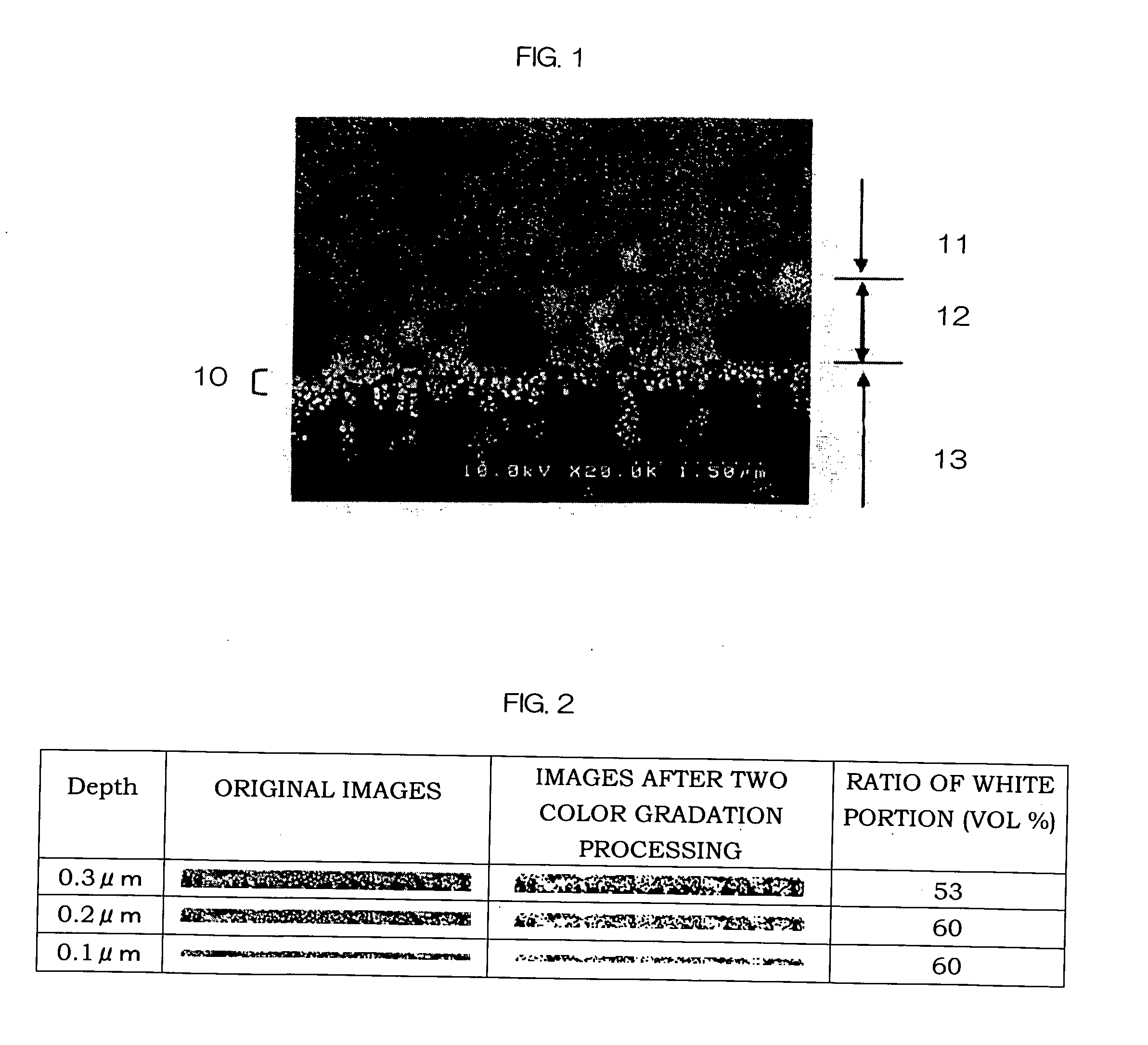
[0274]The Rz of the base material, polyimide film, as determined by measuring the surface in the range of 40 μm×40 μm according to the above-described conventionally-known method and by using NANOPICS 1000 (trade name, manufactured by Seiko Instruments Inc.) was 15 nm. When the surface of substrate A having an intermediate layer formed on the polyimide film was also meas...
PUM
| Property | Measurement | Unit |
|---|---|---|
| width | aaaaa | aaaaa |
| thickness | aaaaa | aaaaa |
| thickness | aaaaa | aaaaa |
Abstract
Description
Claims
Application Information
 - R&D Engineer
- R&D Manager
- IP Professional
- Industry Leading Data Capabilities
- Powerful AI technology
- Patent DNA Extraction
Browse by: Latest US Patents, China's latest patents, Technical Efficacy Thesaurus, Application Domain, Technology Topic.
© 2024 PatSnap. All rights reserved.Legal|Privacy policy|Modern Slavery Act Transparency Statement|Sitemap